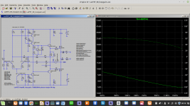
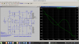
I took the basic Hitachi MOSFET circuit and added various improvements from the Doug Self "Blameless" approach. Output inclusive compensation was one notable idea I thought would help push up the loop bandwidth and make up for MOSFET output non-linearities.
The results seem encouraging:
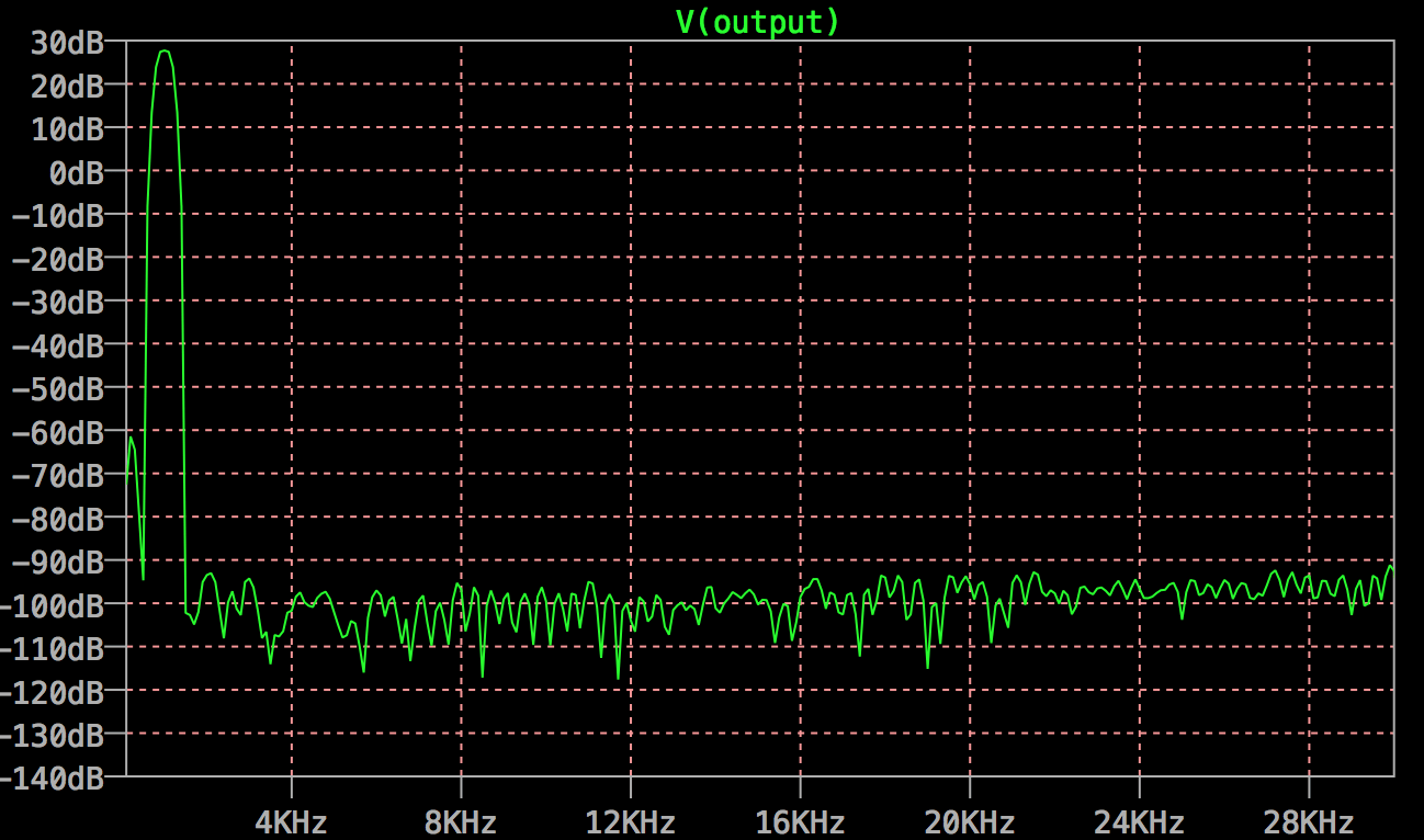
The rails are generated from simulated filtered ac supply and have 1V injected signals to investigate PSRR.
The response curve is nice and flat in the audio band:
The results seem encouraging:
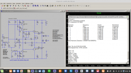
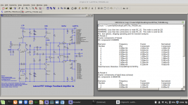
Code:
1 kHz, upto 20 harmonics
========================
Fourier components of V(output)
DC component:-0.0651619
Harmonic Frequency Fourier Normalized Phase Normalized
Number [Hz] Component Component [degree] Phase [deg]
1 1.000e+3 3.433e+1 1.000e+0 0.09° 0.00°
2 2.000e+3 7.955e-5 2.317e-6 -163.36° -163.45°
3 3.000e+3 8.903e-5 2.593e-6 160.10° 160.01°
4 4.000e+3 9.554e-5 2.783e-6 -161.54° -161.63°
5 5.000e+3 1.245e-5 3.625e-7 163.92° 163.83°
6 6.000e+3 7.819e-5 2.277e-6 164.35° 164.26°
7 7.000e+3 3.341e-5 9.732e-7 -137.91° -138.00°
8 8.000e+3 2.837e-5 8.262e-7 118.95° 118.86°
9 9.000e+3 6.566e-5 1.912e-6 164.86° 164.77°
10 1.000e+4 2.677e-5 7.798e-7 -111.55° -111.64°
11 1.100e+4 4.447e-5 1.295e-6 95.35° 95.26°
12 1.200e+4 4.828e-5 1.406e-6 -167.08° -167.17°
13 1.300e+4 9.506e-6 2.769e-7 -113.02° -113.11°
14 1.400e+4 3.214e-5 9.361e-7 115.56° 115.47°
15 1.500e+4 2.929e-5 8.530e-7 -146.44° -146.53°
16 1.600e+4 2.676e-5 7.793e-7 -29.93° -30.02°
17 1.700e+4 4.713e-5 1.373e-6 154.82° 154.73°
18 1.800e+4 3.719e-5 1.083e-6 -117.86° -117.95°
19 1.900e+4 3.332e-5 9.705e-7 10.27° 10.18°
20 2.000e+4 3.624e-5 1.056e-6 -173.58° -173.67°
Total Harmonic Distortion: 0.000649%(0.000000%)
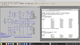
10 kHz, upto 5 harmonics
========================
Harmonic Frequency Fourier Normalized Phase Normalized
Number [Hz] Component Component [degree] Phase [deg]
1 1.000e+4 3.433e+1 1.000e+0 -0.32° 0.00°
2 2.000e+4 4.600e-4 1.340e-5 6.05° 6.38°
3 3.000e+4 4.738e-4 1.380e-5 83.50° 83.83°
4 4.000e+4 5.676e-4 1.653e-5 -95.35° -95.02°
5 5.000e+4 5.736e-4 1.671e-5 116.27° 116.59°
Total Harmonic Distortion: 0.003037%(0.000000%)The rails are generated from simulated filtered ac supply and have 1V injected signals to investigate PSRR.
The response curve is nice and flat in the audio band:
Attachments
I received a convolute of 2SK135/J50 and, after 40 years, I am tinkering with a similar approach using LTSpice.
I wonder that R19 ends at the output - I have a similar compensation scheme with R19 ending at gnd.
I wonder that R19 ends at the output - I have a similar compensation scheme with R19 ending at gnd.
to be honest - not at all.Very nice. But is such a high bandwidth desirable in an audio amplifier?
But it is just fun to improve the numbers...
If you want to push linearity to the limits it is a good idea to begin measurements without load. Doing so I discovered that there is plenty room for improvements around the VAS stage.
Last edited:
Maplin did a copy of the Hitachi datasheet circuit as well.
Many hundreds or possibly thousands sold.
I did a version myself adding current source at front, transistor instead of diode current mirror and front end decoupling. Sounded very good and zero hum with input shorted.
Many hundreds or possibly thousands sold.
I did a version myself adding current source at front, transistor instead of diode current mirror and front end decoupling. Sounded very good and zero hum with input shorted.
in case you're still looking for ideas to play with, you may find some fruit in reviewing Damir's latest efforts here:
120W CFA with lateral MOSFET outputs
mlloyd1
120W CFA with lateral MOSFET outputs
mlloyd1
Very nice. But is such a high bandwidth desirable in an audio amplifier?
No, you want to prefilter the input to remove out of band frequencies, but for the amplifier itself the high bandwidth is what enables the feedback loop to linearize higher frequency audio components so well - the intermodulation at 15k and above is pretty low as a result.
Putting a strong 50+kHz signal into the amp will simply fry the Zobel resistor, not a good idea.
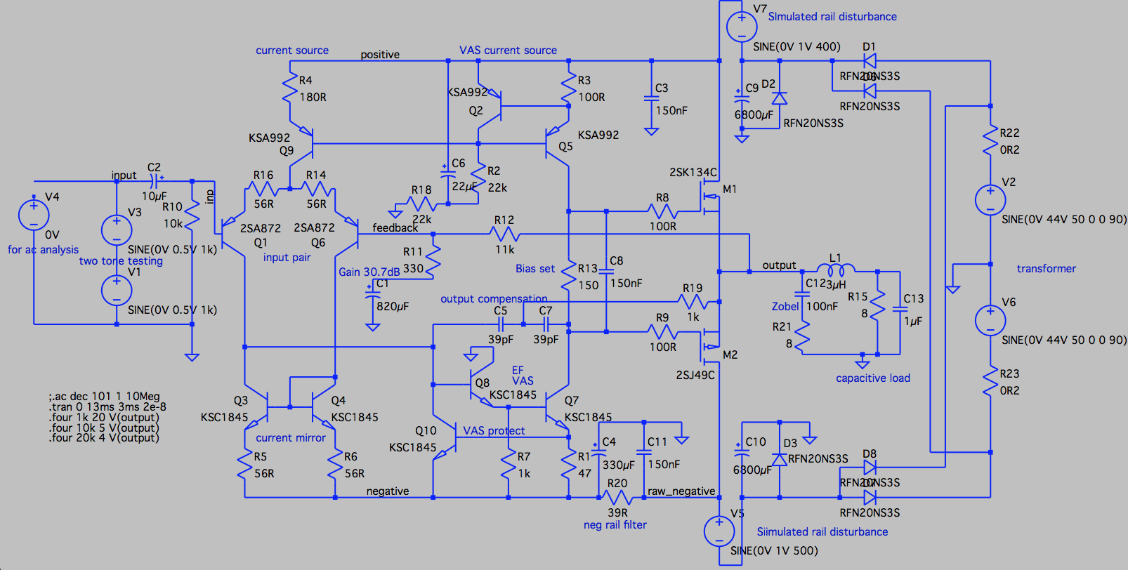
[ The IM between 15kHz and 18kHz tones:

Last edited:
If you want to push linearity to the limits it is a good idea to begin measurements without load. Doing so I discovered that there is plenty room for improvements around the VAS stage.
One thing I noticed is the speed-up capacitor in the VAS chain mustn't be too small or too big, both intruduce more distortion according to my (virtual) experimentation.
Of course with high bandwidth circuits the proof is in the breadboarded version, I suspect that stability issues will crop up that aren't adequately simulated.
totally agreed - theses simus are quite optimistic.One thing I noticed is the speed-up capacitor in the VAS chain mustn't be too small or too big, both intruduce more distortion according to my (virtual) experimentation.
Of course with high bandwidth circuits the proof is in the breadboarded version, I suspect that stability issues will crop up that aren't adequately simulated.
that is what LTSpice promises actually
Attachments
After tinkering with LTSpice for several weeks I will update my work in progress. Nothing really new, but loads of finetuning circuit details.
Attachments
I don't get how the LTP and VAS current sources work. In my opinion they may share a common voltage reference. but in your schematics I'm afraid they'll interact heavily.
Best regards!
Best regards!
I don't get how the LTP and VAS current sources work. In my opinion they may share a common voltage reference. but in your schematics I'm afraid they'll interact heavily.
Best regards!
Hmm, I do not get what makes this part special...
Can you check with LTSpice? This is extremely helpful in analyzing circuitry.
Ok, I think I've got it: The VAS current source is a ring of two. The voltage at Q2's collector/Q5's base is 2 x Vbe wrt the positive supply. This also acts as the reference voltage for the LTP CCS.
Best regards!
Best regards!
Ok, I think I've got it: The VAS current source is a ring of two. The voltage at Q2's collector/Q5's base is 2 x Vbe wrt the positive supply. This also acts as the reference voltage for the LTP CCS.
Best regards!
There is a potential problem at clipping where Q2 saturates and all the current to R14 has to come from the base and R6, which turns off the LEDs. There are too many missing models for me to run the simulation to be sure this actually happens. I normally put a resistor in the base of ~Q2 so that if there is no collector current, the base current doesn't completely steal the current from reference voltage, or use a separate reference voltage. The cap C6 helps for a few microseconds.
I notice that the ~4V LED reference, cascode VAS and drivers, and lateral FETs saz that you don't care about wasting voltage swing and power efficiency. I suppose its better than a class-A efficiency.
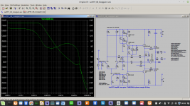
I took the basic Hitachi MOSFET circuit and added various improvements from the Doug Self "Blameless" approach. Output inclusive compensation was one notable idea I thought would help push up the loop bandwidth and make up for MOSFET output non-linearities.
The results seem encouraging:
The rails are generated from simulated filtered ac supply and have 1V injected signals to investigate PSRR.
The response curve is nice and flat in the audio band:
You probably realize this:
1. the "VAS protection" is unnecessary in this circuit because there is no output protection that could shift the load to the VAS. ( but see #5)
2. When the amp clips +V, Q5 base current will try to feed R3 without any collector current and that will interfere with the Q9 base voltage. I put a resistor in the base of Q5 to limit this effect to less than the total current from R2.
3. a small cap directly on the base of Q9 improves the collector impedance of Q9. I usually add a resistor in series with the collector of Q9 for the same reason.
4. A capacitor directly on the base of Q5 , OR, a resistor in the base of Q2 guarantees stability of the current source feedback.
5. The collector of Q8 should be fed by a resistor or divider to limit the Q8 current during -ve clipping and reduce the Q8 collector voltage to allow using faster, cheaper transistor at Q8. This also improves "rail sticking".
6. a small cap on the base of Q1 filters ultrasonic input and improves the feedback pole at Q1 for better phase margin.
7. Tweaking the value of R7 can improve THD. 1K is a bit low.
8. Q2 creates a negative tempco at R13. Is that deliberate?
9. A Zobel network should not be necessary on a follower output. Normally a Zobel network is feedback compensation for CFP outputs.
10. A shunt resistor on L1 keeps the self resonance and C13 resonance under control in all situations, ie no load connected.
I would run your simulation to improve my comments but that would require adding all the missing models so forgive me for being lazy.
Cheers,
Steve
It is always a compromise - this amp is not intended for efficiency, but for "academic" performance. Maybe I add some bootstrapped driver supply to increase output level.
I merged the cordell models and other 3rd party models into my "standard.bjt". So if you replace your "standard.bjt" by mine, you should have all models required
I merged the cordell models and other 3rd party models into my "standard.bjt". So if you replace your "standard.bjt" by mine, you should have all models required
- Status
- Not open for further replies.
- Home
- Amplifiers
- Solid State
- Blameless style lateral MOSFET amp