Hi,
I’m going to build an amp based on the Douglas Self and Randy Slone’s designs form buildaudioamps.com, (http://buildaudioamps.com/project-61/).
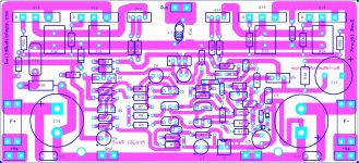
The designer has an image of the PCB that has both the foil and component graphics. I just want the foil side. I’m not an expert manipulating images to make a PCB.
Is there a standard or easy method to isolate the layers so I can use the image to make a PCB?
I’ve attached the image.
Thank you for your advice - az
I’m going to build an amp based on the Douglas Self and Randy Slone’s designs form buildaudioamps.com, (http://buildaudioamps.com/project-61/).
The designer has an image of the PCB that has both the foil and component graphics. I just want the foil side. I’m not an expert manipulating images to make a PCB.
Is there a standard or easy method to isolate the layers so I can use the image to make a PCB?
I’ve attached the image.
Thank you for your advice - az
Attachments
You can't without quite a lot of work in a paint package. Maybe send a message to the site owner and he might send you the appropriate files.
Thank you for your reply.
I wrote him a few days ago but haven't heard anything. I was going to use Christmas break to do some work on the amp.
I wrote him a few days ago but haven't heard anything. I was going to use Christmas break to do some work on the amp.
Last edited:
I was going to use Christmas break to do some work on the amp.
You need the Gerber files to make a pcb.
They also contain the necessary hole size information.
I was hoping for a black and white image or PDF. I was going to use a heat transfer method and drill by hand on the drill press.
I was hoping for a black and white image or PDF.
You can get a pdf from a scanner.
He made the board by etching, so there are no Gerber files available.
Last edited:
If you can't get the ExpressPCB file or the .pdf file from buildaudioamps, you could just use software to convert the PCB image to black and white and manually erase the black lines (the silkscreen) you don't need. It probably wouldn't take more than a half-hour or so.
Resize the image to the correct board size (or pin spacing).
You might have to flip/'mirror' the image.
But getting the image file from the author would be easiest Are they selling the project?
That would explain the posting of a different image from the one they used to laser toner the board.
Resize the image to the correct board size (or pin spacing).
You might have to flip/'mirror' the image.
But getting the image file from the author would be easiest Are they selling the project?
That would explain the posting of a different image from the one they used to laser toner the board.
He doesn't sell a kit or the PCBs. I haven't heard back from him regarding a usable image.
I'm going to have to find a easy to learn paint program.
Thank you
I'm going to have to find a easy to learn paint program.
Thank you
Once it becomes a standard graphic file, such as a .GIF, .PNG, .JPG, etc. you don´t have layers any more, just everything mixed together, and to boot, as a Bitmap, not a Vector file , which is what a PCB type format file actually is.
So much so that even if you find and use the original software used by original designers, not even it can separate it back into layers.
Best you can do , as suggested above, is to blow the image real large (4x to 8X original sizen at least) , then enlarge it a lot so a little bit fills your screen and you manually edit it in a bitmap type graphics package (such as Photoshop).
The tool which will separate layers, correct colours, erase annoying and distracting graphic elements and finally give you just a pure black on white image , period, suitable to print as a transparency and expose a photopositive emulsion clad PCB (excellent results) or Laser thermal transfer (hobbyist grade results) is nothing more or less than your own brain (and lots of patience).
No software I know can do that unaided.
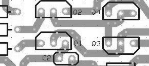
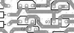
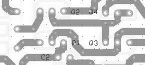
This is a free sample working on just a tiny part of the image.
It was successively grayscaled, reduced to 16 gray depth, black on gray turned into track gray, black on white tuned into white, all grey remaining (2 shades of it remaining) turned into black, silkscreen black turned into white, 16 grey palette edited into either black track or pure white background, at which point it *LOOKS" like a black on white exposure or transfer original.
You still have to remove, pixel by pixel, annoying random dots (probably digital noise embedded in original picture) and traces of silkscreen.
As fun as smashing your own hand with a hammer 😉
But yes, it *can* be done.
Attachments


Thank you very much for this, Mr. JMFahey.
What program are you using to reduce to the 16 gray?
I've started the process with Irfanview and MS Paint. MS Paint is very crude and the pixels are large, so the lines aren't smooth. It's been extremely tedious. I'm already about 4 hours into experimenting, removing and cleaning.
The amp uses an electrolytic cap for its input. That makes me wonder if the amp is actually a good design. I have read that both Randy Slone and Douglas Self's designs are remarkably good.
Thank you again and best to you - z
You´re welcome.
IrfanView is excellent to .... ummm ... "view" images 😉 , but not to edit them.
Any "Photoshop type" software will do, I use prehistoric Paint Shop 4.12 which is shareware so it can legally be used, but I guess ¿Inkscape? is a way more powerful and modern open source program.
Problem is, once you enlarge the images, you painfully see the ragged edge pixels ... because that´s what you actually have there.
There are a couple PCB packages which allow you to import a semi transparent bitmap image (like the one you posted) and redraw a proper PCB over it; it saves a lot of time but, much more important, can be edited whenever you want.
Plus having sharp edges and even generating Gerbers for outsourced fabrication if you wish.
ALL have the same problem: tedious, slow, and fully depend on your brain process, to separate chaff from wheat.
I don't know what JMFahey used, but there's a free Photoshop-like program named Gimp, but like Photoshop it has lots of features and thus a longer learning curve than MS Paint or Irfanview. I use Gimp mostly to crop and resize photos, and it took some time to find the right tools on it just to do that.
ETA: Inkscape is a whole different type of tool - it's vector based and comparable to Adobe Illustrator. It's not what you want to use to manipulate a bitmap image.
Also, the "PCB packages" all have their own learning curve, but if you're wanting draw PCBs to have them made, it's (kinda sorta) worth learning one that outputs the previously mentioned Gerber files, as that's the file format all the PCB manufacturing places accept.
Last edited:
Go buy a PCB from Doug Self and help an engineer make a buck. The Signal Transfer Company
Very pricey, IMO...so more than one buck, for sure.
Very pricey, IMO...so more than one buck, for sure.
Pricey compared to what? You are getting the design and best layout known for that circuit checked and tested by the original designer. If you value your time at $10/hr you are not going to layout and fab an equivalent PCB for less than you can buy from Self.
Pricey compared to what he's paying to have them made.Pricey compared to what?
Pricey compared to other designers' PCBs (Millett, George@tubelab).
$70 (plus shipping) for a PCB??
Not sure where you are looking. I found PCB009 Compact Blameless Power Amplifier. PCB & Set of Construction Notes
£23.00 ea, that's about $29 USD today. For an amplifier design, construction notes and a PCB.
Tubelab.com wants $35 for a PCB "The boards that I currently stock are available for $35 USD each."
£23.00 ea, that's about $29 USD today. For an amplifier design, construction notes and a PCB.
Tubelab.com wants $35 for a PCB "The boards that I currently stock are available for $35 USD each."
Last edited:
Pricey compared to what he's paying to have them made.
Pricey compared to other designers' PCBs (Millett, George@tubelab).
$70 (plus shipping) for a PCB??
This $70 number was WRONG.
I was looking at this one, and mis-remembered the cost.
From the Self website:
The Signal Transfer Company: Price list
PCB003
Precision Preamplifier: PCB, build notes, post & packing:
£129.00 ea
That postage is only within the UK, BTW.
So, it's actually $160 USD plus shipping or $220CAD plus shipping for that PCB; others on the same website are cheaper.
Perhaps that line is a typo error and should be 29 UKP not 129??
Last edited:
- Status
- Not open for further replies.
- Home
- Design & Build
- Construction Tips
- How do I isolate the layers form an image to make a PCB?