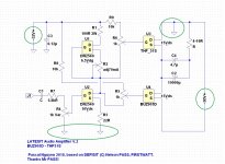
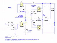
OK Pascal, I understand now that the circuit needs 'two separate power supplies'.
Two supplies are stacked, with (-) of 32V grounded and (+) of 30V grounded, and I don't understand how the THF bias is formed.
THF Gate voltage is higher than its Drain. Forgive and correct me if I am wrong.
Two supplies are stacked, with (-) of 32V grounded and (+) of 30V grounded, and I don't understand how the THF bias is formed.
THF Gate voltage is higher than its Drain. Forgive and correct me if I am wrong.
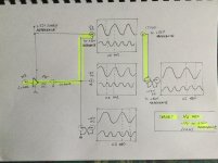
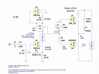
this is the only schm i can understand after two coffee , i will build it first when
i will received all the parts ..🙂
OK Pascal, I understand now that the circuit needs 'two separate power supplies'.
Two supplies are stacked, with (-) of 32V grounded and (+) of 30V grounded, and I don't understand how the THF bias is formed.
THF Gate voltage is higher than its Drain. Forgive and correct me if I am wrong.
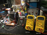
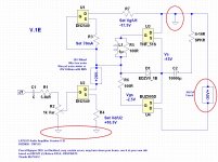
Step two:
Mount 2 Sits and 2 Laterals to heatsink. (Precaution anti static, grounded soldering iron tip, temporarily shorted Sit gate-source).
1.a Connect BUZ905D Drain-Source to 15V3A power supply
1.b Adjust Gate-Source with 0-9V variable to reach 2A.
Lock and record the value of BUZ Vgs@2A
2.a. Connect BUZ905D and THF-51S according to the schéma.
2.b. Connect +30 to chassis and -30 to BUZ’s drain.
2.c. Connect BUZ’s gate-source to the locked variable 0-9V supply.
2.d. Connect Sit’s gate-source with a second variable 0-9V supply and adjust it until both transistors have an equal 15V Drain-Source.
Record that value.
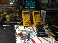
Hope the photos attached is much easier to communicate.
Cheers
.
Attachments

Last edited:
this is the only schm i can understand after two coffee , i will build it first when
i will received all the parts ..🙂
This bias scheme is a shamelessly stolen from the DefiSit schéma, if you add a transformer and a pair 2sk & 2sj, you will have a SIT3.
Cheers
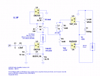
OK Pascal, I understand now that the circuit needs 'two separate power supplies'.
Two supplies are stacked, with (-) of 32V grounded and (+) of 30V grounded, and I don't understand how the THF bias is formed.
THF Gate voltage is higher than its Drain. Forgive and correct me if I am wrong.
...
Once the Vs is half the Vsupply, in my case which is -15V.
The SIT bias would be:
Vbias = Vhalf + Vgs SIT
(-15) + (-2.74) = -17.74
Then the result explains why THF gate voltage is higher than its drain (we are dealing with positive ground).
I am making up (pure amateurism, hihi) any circuit that would amplify an audio signal in its square law with H2 négatif having a minus 17.74V of potentially output for THF-51S and BUZ105D gates.
Cheers

If you connect the (+) of the "32V supply" to ground then it makes sense. Currently 32V (-) is grounded. ^^
If you connect the (+) of the "32V supply" to ground then it makes sense. Currently 32V (-) is grounded. ^^
A bit of 3 steps involved in a signal transformation from audio source to drive the SIT with (-)17V referred to (+)32V supply while providing an H2 negative.
This (-)17V referred will provide a necessary biasing voltage for the output stage
Cheers
.
Attachments
Pascal,
Thank you for your explanation.
But please know that my knowledge is too low to understand the 2nd harmonics formation. I am at the level of barely understanding the static status of voltage distribution.
Looking at your circuit there are two supplies and 32V supply is on top of 30V supply. By grounding the (+) of 30V supply, the bias voltage points (R6 and R7) are above any pin of THF BUZ. This is blocking my understanding, not to mention the 2nd harmonics. 😕
Cheers
Chul
Attachments
Last edited:
If you can show the voltage of each point of the active components pins with reference to the ground symbol, that would help. 🙂
If you can show the voltage of each point of the active components pins with reference to the ground symbol, that would help. 🙂
My bad, got an error on schematic drawing that led you to confuse.
Cheers
Attachments
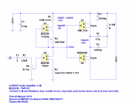
now is simple - two PSUs are connected on their pluses , smaller one is grounded , while bigger one is groundless (no need for , load being referenced to plus side of PSU)
Poor brain
Not yet, dear Colleagues
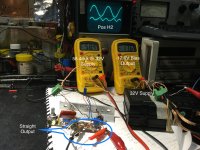
Here is my favourite due to mechanical simplicity for mounting the SITs and using lithium batteries with BMS to power the driver.
Cheers
.
now is simple ...
Now that begin to make sense to my poor brain. 🙂🙂
Not yet, dear Colleagues
Here is my favourite due to mechanical simplicity for mounting the SITs and using lithium batteries with BMS to power the driver.
Cheers
.
Attachments
In the circuit, the battery polarity and its voltage are additional questions to me..
Here is my answer
Have a nice weekend.
.
Attachments
Eureka , now it is as undersandable as a ZM circuit !😀
well, not to ZM

- Home
- Amplifiers
- Pass Labs
- LateSit