Serge, It is a great job and your pdf is nice, I am appreciated. I used to have Dexa’s regs, they are ok, and easy to solder into the place. But I still convinced, that opa based AVCC supply suggested by Mark (based on the ESS paper) is a superior solution. Also, to build the circuit is not as cost effective as the New Class D Dexa’s are (2x37 €) - even using the LTC6655 as a 3.3V reference. So I recommend to put Mark’s AVCC version into the page 4-6 including LTC6655 (as an upgrade to the LT1763s).
Last edited:
Serge, It is a great job and your pdf is nice, I am appreciated. I used to have Dexa’s regs, they are ok, and easy to solder into the place. But I still convinced, that opa based AVCC supply suggested by Mark (based on the ESS paper) is a superior solution. Also, to build the circuit is not as cost effective as the New Class D Dexa’s are (2x37 €) - even using the LTC6655 as a 3.3V reference. So I recommend to put Mark’s AVCC version into the page 4-6 including LTC6655 (as an upgrade to the LT1763s).
Thanks janos-904
New Class D Dexa’s are (2x37 €) .....look at PartsConnexion 14$ !!! each
Serge
Hi Guys, Thank you for all the thoughtful posts. I have a busy day today, but have started thinking about possible through hole solutions. Will see about responding in more detail later.
Where does one purchase a ES9038Q2M chip. Just the chip? I can't seem to find it for purchase even on the ESS site.
There is a list of distributors at the ESS website. They can sell parts and provide data sheets.
ES9038PRO full balanced decoder supports the DSD256 DOP PCM384K XMOS HiFi DAC | eBay
Didn't take long did it? Not commenting on implementation but the idea of using digital reconstruction is there now. Altera FPGA and do I see an ARM processor there as well?
Didn't take long did it? Not commenting on implementation but the idea of using digital reconstruction is there now. Altera FPGA and do I see an ARM processor there as well?
Where does one purchase a ES9038Q2M chip. Just the chip? I can't seem to find it for purchase even on the ESS site.
ES9028Q2M (2 CHNL) New - Shaw Electronics
Another one. This time Digital reconstruction as well as ESS9311 regs!!!
SMSL VMV D1 PURE DAC DUAL ES9038PRO XMOS XU208 USB DSD512 768KHZ OPTIC COAXIAL | eBay
SMSL VMV D1 PURE DAC DUAL ES9038PRO XMOS XU208 USB DSD512 768KHZ OPTIC COAXIAL | eBay
Sounds like any DAC purporting to be up there and using Sabre chips will need that. AGain not saying these are good dacs but the key elements are now being adopted and maybe competition will have some trickle down effect in time.
Weiliang ES9038PRO DAC Asynchronous USB DAC Decoder 384K DSD256 + Headphone amp | eBay
First time I've seen this done on an Ebay Board. They appear to be using complementary 2N5401 and 2N5551 transistors on the output of the single op amps . I would think they want to beef up the output of the op amp for loading reasons. Now this is being done prior to the last stage of the Balanced to Single Ended stage. They are using single op amps throughout the low cost board which is also a rarity. The OPA604 is already rated to drive 600ohm loads so interesting why they would need to beef up the output prior to single ended. Was Abraxalito onto something when he discussed loading of the op amps? They also appear to be using LEDs for biasing as well. I have not seen Ebay boards doing this before.
First time I've seen this done on an Ebay Board. They appear to be using complementary 2N5401 and 2N5551 transistors on the output of the single op amps . I would think they want to beef up the output of the op amp for loading reasons. Now this is being done prior to the last stage of the Balanced to Single Ended stage. They are using single op amps throughout the low cost board which is also a rarity. The OPA604 is already rated to drive 600ohm loads so interesting why they would need to beef up the output prior to single ended. Was Abraxalito onto something when he discussed loading of the op amps? They also appear to be using LEDs for biasing as well. I have not seen Ebay boards doing this before.
Doesn't look to me like they have figured it out yet. Don't know what the FPGA is supposed to be doing. Some of it looks like marketing fluff. I'll believe they know what they are doing for SQ when I see comprehensive measurements along with listening tests. Don't think they are ready for that kind of scrutiny yet.
What would lead you to conclude they have not figured it out yet? That is an assumption - could be true and probably is.... but it is nonetheless an assumption Mark. That is dangerous reasoning.
FPGA DACs - DAC - Digital to Analog Conversion - Computer Audiophile
A lot of ways to use them things.
A lot of ways to use them things.
What would lead you to conclude they have not figured it out yet?
I looked at the pictures and read the claimed specs. After awhile you learn some things about how these Sabre-based dacs work. Different problems for each of the dacs you linked to.
Tomorrow I will see if I can take some initial steps to get working on a though-hole output stage layout. Before I go too far with it though I may want to post some pictures and get a feel for what people think about the level of difficulty for some different options. For example, when it comes to AVCC it would be nice to have the option of using an LT6655. Unfortunately, it is SMD and rather small SMD at that. However, it should work okay on one of those little SMD adapter boards various people make. Another example might be that the existing dac board output stage opamp socket and SMD component solder pads could be reused for differential summing and filtering after through-hole I/V stages. Would that be something people would be okay with, or do they need through-hole differential summing to go with the through-hole I/V?
Last edited:
Hi Mark, Very nice de to read that you will try to make a simple and visual tutorial about I/V stage.
For me it is a good way to go to determine what I am able to acheive.
Before I go too far with it though I may want to post some pictures and get a feel for what people think about the level of difficulty for some different options.
For me it is a good way to go to determine what I am able to acheive.
Tomorrow I will see if I can take some initial steps to get working on a though-hole output stage layout. Before I go too far with it though I may want to post some pictures and get a feel for what people think about the level of difficulty for some different options. For example, when it comes to AVCC it would be nice to have the option of using an LT6655. Unfortunately, it is SMD and rather small SMD at that. However, it should work okay on one of those little SMD adapter boards various people make. Another example might be that the existing dac board output stage opamp socket and SMD component solder pads could be reused for differential summing and filtering after through-hole I/V stages. Would that be something people would be okay with, or do they need through-hole differential summing to go with the through-hole I/V?
I'd really rather you did something that was more focused on 80% performance / 20% absolute ease of building. Even if that means adopting some SMD components.
We're a pretty OCD/mod-happy group and I think there will end up being mods to your IV design if too much performance is abandoned in the desire to make it all through-hole. 🙂
After all of these mods to the original board and this upcoming IV stage, I'd almost think it might make sense to start designing an open-source PCB of our own we can get made for both stages. That'd be the dream.
Thanks again for doing this too, and all the work you've put into this thread. I'm excited to see how this turns out.
Okay then, my preference would be to reuse the existing output stage real estate for the new differential out as I did on my own modded dac, but with better filtering.
As far as the I/V part goes, that would take two dual opamps, one for each channel. If a through-hole differential stage was wanted it could go next to the I/V opamps.
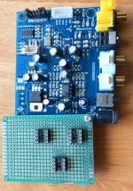
Two pictures below show a quick and dirty mock up of an external output stage with enough space on it both I/V opamps and for the differential output, which would be the third dual opamp.
On the bottom of the board is a conceptual mock up of a ground plane connected as an extension to the existing dac ground plane (note: there are some missing gaps in the ground plane which should actually be more continuous) . Where the mock up ground plane crosses a power trace on the dac board, that could either be insulted with Kapton tape, or the trace removed.
Anybody have any comments on the general concept?
As far as the I/V part goes, that would take two dual opamps, one for each channel. If a through-hole differential stage was wanted it could go next to the I/V opamps.
Two pictures below show a quick and dirty mock up of an external output stage with enough space on it both I/V opamps and for the differential output, which would be the third dual opamp.
On the bottom of the board is a conceptual mock up of a ground plane connected as an extension to the existing dac ground plane (note: there are some missing gaps in the ground plane which should actually be more continuous) . Where the mock up ground plane crosses a power trace on the dac board, that could either be insulted with Kapton tape, or the trace removed.
Anybody have any comments on the general concept?
Attachments

Last edited:
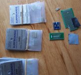
Thought I might see if I could post some pictures of some SMD resistors and give some idea of how to solder them to regular perfboard or adapter boards for SMD. I am trying to show that it is nothing to be afraid of. Just try it with a practice kit or some junk parts to get a feel for what it is like to do it.
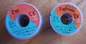
Also, wanted to show 0.3mm and 0.4mm diameter solder I use. It is important to use the correct diameter solder. Small joints need small solder and small solder iron tips. Large joints need larger items. In addition, it can help a whole lot to make sure your solder is clean and not oxidized. Just wipe it gently with a paper towel until all or most of the gray color stuff comes off. Then it is ready to give to a good easy joint. It is much harder to get oxidized solder to flow and solder well.
Besides clean, small diameter solder and a clean, small tip (use a clean brillo pad type tip cleaner such as Hakko, get some refills too), the only other issue is how to hold parts in place while soldering. You can tape as I show here, you can put some solder on a pad then use tweezers to bring the SMD part down to the pad and stick it into the molten solder, you can make a gizmo thing like I did to hold down parts. If you have an assistant you can call on as a third hand to feed solder or hold a part with tweezers that can work too. Just figure out what works for you.
Okay, with that do we any comments or questions about SMD like in the pictures below? Does it still look scary? (Please respond otherwise I have no idea what you think.)
Attachments

Last edited:
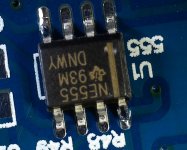
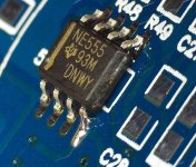
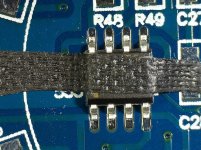
I wanted to show how to solder an IC with multiple pins. The usual way is to solder one corner first, make sure it looks okay and fix it if not okay. Once it is okay with one pin then solder the opposite corner. After that the rest of the pins can be soldered.
To illustrate what might happen and how to fix it, I also intentionally messed up some of the pins, then used solder wick and then alcohol to clean them up. The way I use the wick is to lay it across all affected pins, then use the flat side of the iron tip to heat the strip of wick and all the pins at once. After cleaning them up they were resoldered properly.
Also made a movie of soldering the 1st pin. You can see me try to rotate the solder iron tip a little which sometimes helps. Sometimes a lot of rotation can help even more. The move is at my Dropbox, but can't say for how long. If someone else wants to host it that would be fine. Link is here: Dropbox - SMD Solder.MOV
Attachments


Last edited:
- Home
- Source & Line
- Digital Line Level
- ES9038Q2M Board