http://www.diyaudio.com/forums/parts/35821-some-noise-measurements-leds-zener-diodes.html
and with 1% R we expect better than -30 dB CM to Diff conversion in the mirrored diff pair shown
at 0.3 uV in a 20kHz BW the 12V Zener noise needent be an issue
higher Vz gives lower normalized noiseBZX55/C12 (0.5W 12V):
#1 @ 1mA: 0.35 0.37 0.37 0.39 0.39 uV
#1 @ 5mA: 0.30 0.28 0.28 0.28 0.30 uV
#1 @ 20mA: 0.24 0.25 0.25 0.26 0.25 uV
#2 @ 1mA: 0.32 0.33 0.32 0.33 0.32 uV (Vr = 11.32 V)
#2 @ 5mA: 0.26 0.26 0.27 0.32 0.26 uV (Vr = 11.37 V)
#2 @ 20mA: 0.25 0.26 0.28 0.24 0.30 uV (vr = 11.42 V)
and with 1% R we expect better than -30 dB CM to Diff conversion in the mirrored diff pair shown
at 0.3 uV in a 20kHz BW the 12V Zener noise needent be an issue
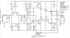
Note that Mooly post20 has added an output Zobel (R20+C3).
This is compulsory. You can change the values slightly, but you need both the R and the C parts.
He has also added the output inductor. This is optional, but highly recommended.
It needs a damping resistor in parallel. Try 1uH||5r
again you can change the component values slightly, but do include the damping resistor.
I suggest you change Q14 & Q15 to a matched pair of BC550c.
Q15 operates with a Vce = ~600mV and the 2n5551 is not very good at doing this.
Q14 should operate at the same Vce to allow it to match it's partner. But the collector voltage is determined by Vbeq12+Vbeq4+Vr6
You can adjust Vceq14 by changing the current in the LTP (not good because that also changes the stability margins) or by changing the values of R18 & R19. These can go up until Vr18 exceeds 600mV and at this level you will find that Vceq14 ~=Vceq15.
You can predict values using the simulator when you ask it the correct questions.
I think Mooly's R24 = 220r is far too small. A value between 5k and 100k (use a temporary trim pot to find the best value on the scope trace) is more likely to to give a nicely rounded squarewave test signal rather than overshoot which can be audible on fast music signals.
Last edited:
Base Stoppers
Add provision for base stoppers to most BJTs.
Outputs, Drivers, Pre-drivers, and CCS pass and control sides.
They can be set to zero with links, or very low, or slightly larger.
Try outputs with 2r2, drivers with 10r and pre-drivers with 47r
Add provision for base stoppers to most BJTs.
Outputs, Drivers, Pre-drivers, and CCS pass and control sides.
They can be set to zero with links, or very low, or slightly larger.
Try outputs with 2r2, drivers with 10r and pre-drivers with 47r
Supply rail Decoupling capacitors.
Post1 shows 15 decoupling capacitors, but little clue to where they are located.
The HF decoupling need to be beside the leadouts of the components which change their currents rapidly and must have a very short loop length to minimise inductance to allow the very fast current changes to flow around the component+decoupling loop.
Thanks for the help everyone.
I have removed the DC offset through changing that resistor and adding the capacitor in the feedback.
Currently the issue is lack of stability with reasonable bias currents. If i increase it any higher than 20mA the amplifier with oscillate heavily with Mooly's compensation scheme.
I tried increasing the C1 (Mooly's schematic) to 100pF in 30pF increments, I gained some stability and manged to get a smooth increase in bias while changing the pot however the amplifier still oscillates just sitting there at 100mA.
As it stands i have Mooly's schematic (form post 20) implemented however with one pair of outputs and 10R base stoppers (lowest value I had above 0R).
Any tips on how to go about finding stability would be wonderful 🙂. Thanks!
you need a scope to look at the overshoot, or lack of, on a 1kHz squarewave.
Have you added the output Zobel?
There should be absolutely no overshoot into a range of resistive loads from rated load all the way up to open load.
There may be a tiny overshoot that damps quickly for a range of capacitive loads in parallel with rated output.
But never an undamped ringing until the transistion to the next half wave.
Adding the capacitive load after the output inductor can give an apparently stable response that is misleading.
I suspect this hidden instability may be why we sometimes get reports of normal working for months and then suddenly a blow up !
Last edited:
I had a look at the output net at post #20
Zobel 0.1uF 10 ohm. Inductor 4uH, Rload 8 ohm.
This gives a band limiting at 250KHz -3dB
What is recommended as a -3dB band limit ?
What do you think about using a 15uH inductor for a band limit at 90KHz. Then, should the Nobel values be changed ?
Actual drivers are far from a resistive 8 ohm load, how do you take care of this about the output net ?
Inserting a 15uH inductor at the 8 ohm load, does improve THD at 20Khz in simulations, however when in the real world, I wonder wether this is not just cosmetic.
Last edited:
the output inductor is generally between 0.5uH and 6uH.
but fashion has brought the upper limit down to ~2uH.
So 0.5uH to 2uH is recommended.
The R needs to be lowish to damp the inductor. <<10ohms is better.
I have seen as low as 1r, but it is exceptional. The Designer may have had mitigating values elsewhere to tolerate this very low value.
We rarely see 3r3, most are 4r7 and higher.
Simulating an actual speaker as the amplifier's load is possible. ESP has a page on this.
Most only use resistive loads and then parallel a simple capacitor to check stability margins.
Most only use resistive loads and then parallel a simple capacitor to check stability margins.
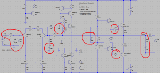
So the circuit as you have it now is looking like this. I'm wondering now, if you have some issues with layout and grounding. It is vitally important that the input ground is not able to be 'contaminated' by the output stage currents. This becomes even more problematic with a stereo pair.
If you have two channels connected up then I would suggest isolating them and working on just one.
Also, the 30pF cap can be increased over 100pF as a way to test and try and force the amp into submission.
The small 15pF cap across the feedback resistor should not be increased, that could make things worse. You can try reducing or omitting that as a test.
Attachments
the resistor next to R15 has a typo.
What happens to performance if R5 (CCS current) is set to between 2k2 and 3k9?
What happens to performance if R5 (CCS current) is set to between 2k2 and 3k9?
Last edited:
Looks good Mooly. I've combinations of the capacitors of the 30pF and 15pF. The 30pF had very little affect up to 1nF (tried in steps). I couldn't improve on the 15pF.
I'm interested to know how changing the bias currently affects the stability of the amplifier.
Attached is a print screen of the output with a 1kHz square wave in with the output bias set low enough for no oscillation to occur when there is no input signal.
I'm interested to know how changing the bias currently affects the stability of the amplifier.
Attached is a print screen of the output with a 1kHz square wave in with the output bias set low enough for no oscillation to occur when there is no input signal.
Attachments

I think so, yes.
In Bobs own words the amplifier is described as 'basic' (at least at the start of the relevant text) and it is then used as a building block to show various techniques.
I wouldn't want to speak for Bob, but I doubt he had it in mind as a completed project ready for the real world. To do that needs a bit of polishing as I have attempted here.
Its all fairly basic stuff, reduce the gain to unity at DC, add a suitable input filter and decide on a suitable input impedance. Attend to the output stage re components required for stability with real loads.
It seems fairly decent as it stands now.
the resistor next to R15 has a typo.
What happens to performance if R5 (CCS current) is set to between 2k2 and 3k9?
Hi AndrewT, I've tried adjusting the value in the range you said but didn't see any difference in stability unfortunately.
the resistor next to R15 has a typo.
What happens to performance if R5 (CCS current) is set to between 2k2 and 3k9?
Very little difference. Even with nearly 3ma per transistor in the LTP and all is still good.
Looks good Mooly. I've combinations of the capacitors of the 30pF and 15pF. The 30pF had very little affect up to 1nF (tried in steps). I couldn't improve on the 15pF.
I'm interested to know how changing the bias currently affects the stability of the amplifier.
Attached is a print screen of the output with a 1kHz square wave in with the output bias set low enough for no oscillation to occur when there is no input signal.
I'm going to stick my neck out and say that the problems you have now are going to be down to physical implementation, in particular interaction between the input ground, the feedback return and the zobel return point.
What we have done so far has been absolutely essential, there is no doubt on that, but we are now seeing practical issues of implementation.
Have you got any load attached in that screen shot ?
(bias current should not materially affect the stability at all. It should be fine from zero bias all the way up to destructively high settings)
http://www.diyaudio.com/forums/parts/35821-some-noise-measurements-leds-zener-diodes.html
higher Vz gives lower normalized noise
and with 1% R we expect better than -30 dB CM to Diff conversion in the mirrored diff pair shown
at 0.3 uV in a 20kHz BW the 12V Zener noise needent be an issue
If you look at the text file attached to the first post of the thread you refer to, you see a quick increase in noise up to 6.8 V and then an enormous improvement between 6.8 V and 12 V:
"Zeners:
---------------------------------------------------------
(All zeners of brand Temic.)
BZX55/C2V7 (0.5W 2.7V):
#1 @ 1mA: 1.1 1.1 1.1 1.1 1.1 uV
#1 @ 5mA: 1.0 0.88 0.85 0.86 0.87 uV
#1 @ 20mA: 1.0 0.81 0.72 0.72 1.1 uV
#2 @ 1mA: 1.2 1.1 1.1 1.1 1.1 uV (Vr = 2.03 V)
#2 @ 5mA: 0.91 0.88 0.87 0.86 0.85 uV (Vr = 2.50 V)
#2 @ 20mA: 1.1 0.80 0.77 0.73 0.71 uV (Vr = 3.02 V)
BZX55/C5V6 (0.5W 5.6V):
#1 @ 1mA: 5.3 5.3 5.3 5.3 5.3 uV
#1 @ 5mA: 2.9 2.9 2.9 2.9 2.9 uV
#1 @ 20mA: 1.7 1.6 1.6 1.6 1.6 uV
#2 @ 1mA: 5.3 5.3 5.3 5.3 5.3 uV (Vr = 5.68 V)
#2 @ 5mA: 2.9 2.9 2.9 2.9 2.9 uV (Vr = 5.77 V)
#2 @ 20mA: 1.8 1.6 1.6 1.6 1.6 uV (Vr = 5.81 V)
BZX55/C6V8 (0.5W 6.8V):
#1 @ 1mA: 16 16 16 16 16 uV
#1 @ 5mA: 21 21 21 21 21 uV
#1 @ 20mA: 5.8 5.5 5.5 5.5 5.6 uV
#2 @ 1mA: 25 25 25 25 25 uV (Vr = 6.93 V)
#2 @ 5mA: 13 13 13 13 13 uV (Vr = 6.96 V)
#2 @ 20mA: 4.6 4.7 4.5 4.5 4.4 uV (Vr = 7.00 V)
(Rechecked both devices due to their inconsistent
behaviour for 1 and 5mA).
BZX55/C12 (0.5W 12V):
#1 @ 1mA: 0.35 0.37 0.37 0.39 0.39 uV
#1 @ 5mA: 0.30 0.28 0.28 0.28 0.30 uV
#1 @ 20mA: 0.24 0.25 0.25 0.26 0.25 uV
#2 @ 1mA: 0.32 0.33 0.32 0.33 0.32 uV (Vr = 11.32 V)
#2 @ 5mA: 0.26 0.26 0.27 0.32 0.26 uV (Vr = 11.37 V)
#2 @ 20mA: 0.25 0.26 0.28 0.24 0.30 uV (vr = 11.42 V)"
During measurements I did myself many years ago I also saw a big increase somewhere around 5 V to 6 V, as expected. I don't remember seeing any improvement at higher Zener voltages, but then again, I don't remember whether I went all the way up to 12 V. I just checked whether I could still find the details in the attic, but with no success.
Anyway, it's all of academic interest as the thread starter did not complain about noise. I would like to know what causes the improvement at 12 V, though. Does anyone know?
not completely irrelevant, if Zener noise isn't a problem then my suggestion of splitting the bias R to decouple for PSR is the better choice over trying to shunt the Zener dynamic R of 10s to maybe 100 Ohms with a C that gives 100 Hz attenuation
You are running a triple OPS - from my experience the decoupling and base stopper requirements are mandatory. Bob Cordell discusses this at length in his book. What you could do just to get you amp going is remove Q16, Q17, C7 and R11 so you amp is then an EF2. You will have to adjust the OPS bias accordingly. These are very forgiving compared to an EF3. If that cleans it up, you need to revisit Bob's write-up on EF3's.
Has anyone suggested a base stopper for Q6? There was a discussion somewhere on the forum on the active current source and its propensity to break into oscillation sans the base stopper in the control (Q6) transistor.
Also, while you are trying to get the amp stable, I would not put the phase lead compensation (R24 and C4) in across the feedback resistor. Reason: If it is chosen carefully, you can get extra phase margin and that is helpful. However, if you overcook it, you put a zero in the feedback loop and that can lead to instability.
I would also suggest you also decouple the base spreader circuit (Q5). I have found 10uF 10V works well.
"Anyway, it's all of academic interest as the thread starter did not complain about noise. I would like to know what causes the improvement at 12 V, though. Does anyone know?"
Marcel, my guess is the current source is oscillating. Base stopper might help or decoupling of the Zener diode
Marcel, my guess is the current source is oscillating. Base stopper might help or decoupling of the Zener diode
If you look at the text file attached to the first post of the thread you refer to, you see a quick increase in noise up to 6.8 V and then an enormous improvement between 6.8 V and 12 V:
"Zeners:
---------------------------------------------------------
(All zeners of brand Temic.)
BZX55/C2V7 (0.5W 2.7V):
#1 @ 1mA: 1.1 1.1 1.1 1.1 1.1 uV
#1 @ 5mA: 1.0 0.88 0.85 0.86 0.87 uV
#1 @ 20mA: 1.0 0.81 0.72 0.72 1.1 uV
#2 @ 1mA: 1.2 1.1 1.1 1.1 1.1 uV (Vr = 2.03 V)
#2 @ 5mA: 0.91 0.88 0.87 0.86 0.85 uV (Vr = 2.50 V)
#2 @ 20mA: 1.1 0.80 0.77 0.73 0.71 uV (Vr = 3.02 V)
BZX55/C5V6 (0.5W 5.6V):
#1 @ 1mA: 5.3 5.3 5.3 5.3 5.3 uV
#1 @ 5mA: 2.9 2.9 2.9 2.9 2.9 uV
#1 @ 20mA: 1.7 1.6 1.6 1.6 1.6 uV
#2 @ 1mA: 5.3 5.3 5.3 5.3 5.3 uV (Vr = 5.68 V)
#2 @ 5mA: 2.9 2.9 2.9 2.9 2.9 uV (Vr = 5.77 V)
#2 @ 20mA: 1.8 1.6 1.6 1.6 1.6 uV (Vr = 5.81 V)
BZX55/C6V8 (0.5W 6.8V):
#1 @ 1mA: 16 16 16 16 16 uV
#1 @ 5mA: 21 21 21 21 21 uV
#1 @ 20mA: 5.8 5.5 5.5 5.5 5.6 uV
#2 @ 1mA: 25 25 25 25 25 uV (Vr = 6.93 V)
#2 @ 5mA: 13 13 13 13 13 uV (Vr = 6.96 V)
#2 @ 20mA: 4.6 4.7 4.5 4.5 4.4 uV (Vr = 7.00 V)
(Rechecked both devices due to their inconsistent
behaviour for 1 and 5mA).
BZX55/C12 (0.5W 12V):
#1 @ 1mA: 0.35 0.37 0.37 0.39 0.39 uV
#1 @ 5mA: 0.30 0.28 0.28 0.28 0.30 uV
#1 @ 20mA: 0.24 0.25 0.25 0.26 0.25 uV
#2 @ 1mA: 0.32 0.33 0.32 0.33 0.32 uV (Vr = 11.32 V)
#2 @ 5mA: 0.26 0.26 0.27 0.32 0.26 uV (Vr = 11.37 V)
#2 @ 20mA: 0.25 0.26 0.28 0.24 0.30 uV (vr = 11.42 V)"
During measurements I did myself many years ago I also saw a big increase somewhere around 5 V to 6 V, as expected. I don't remember seeing any improvement at higher Zener voltages, but then again, I don't remember whether I went all the way up to 12 V. I just checked whether I could still find the details in the attic, but with no success.
Anyway, it's all of academic interest as the thread starter did not complain about noise. I would like to know what causes the improvement at 12 V, though. Does anyone know?
Marcell,
I also did this kind of test using an noise amplifier I showed here in other topic. I got very diferent results from your.
Of couse the zener current is very important and I do not care it in my previous post when I show one simulation file.
For instance, when I analised noise from LM431 it depend from manufacturer and production. So I suppose it could happens to your test.
By the way, an simple RC filter can attenuate a lot the noise spectrum
Sorry for of topic coment.
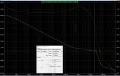
I went ahead and did some loop gain plot with the Tian probe trying to see what the stability margin we could anticipate. Here is my observation.
1. As is
I started out based on Mooly's LTspice schematic in post #20, with an extra 4R7 damping resistor across the output coil, and an extra 0.1uF capacitor across the Vbe multiplier.
The result doesn't look too good with gain margin at about mere 10dB, and some peaking in the amplitude there about.
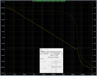
2. C4-R24 network removed.
Saw major improvement in gain margin, now at 35dB, plenty, yet the peaking is still there.
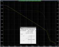
3. damping R-C network put in at pre-driver transistors.
Loop gain Peaking is tamed, gain margin now at 33dB, still excellent.
A few years ago I did some simulation trying to get a handle about the behavior of a 5-pair 3EF output. See this post. Was not surprised to see the notorious peaking in the high frequencies. That simulation shows how the peaking respond to different source impedance, and that it can be tamed with a R-C shunt at its input. That seems to be why the R-C network at the pre-driver transistors worked.
1. As is
I started out based on Mooly's LTspice schematic in post #20, with an extra 4R7 damping resistor across the output coil, and an extra 0.1uF capacitor across the Vbe multiplier.
The result doesn't look too good with gain margin at about mere 10dB, and some peaking in the amplitude there about.
2. C4-R24 network removed.
Saw major improvement in gain margin, now at 35dB, plenty, yet the peaking is still there.
3. damping R-C network put in at pre-driver transistors.
Loop gain Peaking is tamed, gain margin now at 33dB, still excellent.
A few years ago I did some simulation trying to get a handle about the behavior of a 5-pair 3EF output. See this post. Was not surprised to see the notorious peaking in the high frequencies. That simulation shows how the peaking respond to different source impedance, and that it can be tamed with a R-C shunt at its input. That seems to be why the R-C network at the pre-driver transistors worked.
Attachments
- Status
- Not open for further replies.
- Home
- Amplifiers
- Solid State
- Please help with issues I'm having with my Bob Cordell amplifier implementation.