Hi guys please help,
One of my Slewmaster channels is burned off maybe due to a short circuit between ground and a transistor house mounted to main heatsink or driver heatsink.
question is:
For BIAS transistors - Can I use BD139 for one channel and 2SC3423 for the other channel (2SC3423 have complete plastic house) without any difference in soundquality or distortion performance between the two channels?
(If the other channel with BD139 BIAS transitors burns of I will also change thoose to 2SC3423)
Kim
Hi Kim, although 2SC3423 is a better transistor in general, it doesn't matter if it's used as a bias thermal sensor 🙂 It's going to work fine. Virtually any TO-126 will. Complete plastic house is even more convenient - you don't need to bother about some insulation pad.
Cheers,
Valery
Cheers,
Valery
 OT posts moved to
 Kypton ND
Hallo All.
The Kapton ND needs a 4.7uf capacitor on the input. I have a better quality 10uf capacitor that I can use there. Can this be done and is it a goood idea ? 🙂
Hallo All.
The Kapton ND needs a 4.7uf capacitor on the input. I have a better quality 10uf capacitor that I can use there. Can this be done and is it a goood idea ? 🙂
I don't think it is a good idea.
I have the opinion like some others that the two input filters should determine the passband of the amplifier.
All the signal that is passed to the amplifier should be properly processed by the amplifier.
If you widen the input passband you can reach a point where the amplifier cannot handle the signal you are now feeding through the modified filter/s.
If you widen the input passband you can reach a point where the amplifier cannot handle the signal you are now feeding through the modified filter/s.
Can You tell me, what can be problem, if the amplifier get little more 10Hz components? I'm sure, that it can't hurt the amplifier.
Sajti
should be properly processed by the amplifier
I did not saywhere the amplifier cannot handle the signal
hurt the amplifier
I did not say
OK than I try again: Can You please describe, how the amplifier will handle the higher amount 10Hz components improperly?
Sajti
the NFB loop develops voltage across the DC blocking cap and since there is now reduced feedback cannot correct for extra distortion.
And there may be LF instability due to trying to pass LF.
And there may be LF instability due to trying to pass LF.
Thanks Andrew, so I will use 2 x 2,2uf poly caps in parallel. I have 4.7uf electrolytic caps but I'm not sure which is better for the input cap. 😕
Thanks Andrew, so I will use 2 x 2,2uf poly caps in parallel. I have 4.7uf electrolytic caps but I'm not sure which is better for the input cap. 😕
Avoid using electrolytics for the input unless they are the non-polarised types. Stick with the parallel combination of poly caps.
Hari
the NFB loop develops voltage across the DC blocking cap and since there is now reduced feedback cannot correct for extra distortion.
And there may be LF instability due to trying to pass LF.
I did simulation with 10Hz, 5Hz, 2Hz. There was no any DC offset, the distortion was absolutely same.
What can be reason of the LF instability, if it not exist, with smaller input capacitor? The common ss amplifier use only single capacitor at the feedback, which makes not enough phase shift for the oscillation.
Sajti
Thanks Andrew, so I will use 2 x 2,2uf poly caps in parallel. I have 4.7uf electrolytic caps but I'm not sure which is better for the input cap. 😕
You can use 10uF, with no problem! The original 4.7uF gives about 1,5Hz (-3dB), so 10uF gives 0,7Hz. I know many commercial amplifier which use 22uF in same position.
Sajti
Is the amplifier designed to pass this LF without misbehaving?
It is CFP design with capacitor coupled feedback. Feedback LF limit is 3.4Hz (-3dB). Schematic attached.
I have to increase the input level to 7.5V at 1Hz to reach the nominal output level. Distortion is 0.003%
Sajti
Attachments
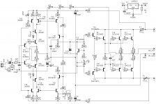
there's the potential problem.It is CFP design with capacitor coupled feedback. Feedback LF limit is 3.4Hz (-3dB). Schematic attached.
I have to increase the input level to 7.5V at 1Hz to reach the nominal output level. Distortion is 0.003%
Sajti
The NFB is entering cut off @ 3.4Hz and yet the input filter is passing down to 0.7Hz.
The DC blocking capacitor is being subjected to AC voltage and that screws with performance.
If you want to keep the 100r and 1mF for R7 & C2 then keeping R51 = 22k6 makes my recommendation for C4 <3uF
Last edited:
R54 seems to be in the wrong place.
Placed as shown it will amplify interference coming in from the source connection.
Placed as shown it will amplify interference coming in from the source connection.
Last edited:
The DC blocking capacitor is being subjected to AC voltage and that screws with performance.
On which frequency? At 3.4Hz? How big is the input level, from a common source at 3.4Hz?
R54 is planned if I build it into integrated amplifier. I not use it if it's only a poweramp.
Sajti
The recommendation for determining the NFB values is:
C2 >= sqrt(2) * C4 * R51 / R7 and for the values shown becomes enormous.
Turning around that recommendation to work back to a value for C4 one would use:
C4 <= C2 * R7 / R51 / sqrt(2) <= 1mF * 100r / 22k6 /1.4 <= 3.1uF
R54 still looks to be in the wrong location.
It is in the signal route and any interference current passing around the input circuit will develop an interference voltage across R54 that adds to the wanted signal.
Is this sch an original from the amp Designer, or has it been modified by some other Builder?
Last edited:

- Home
- Amplifiers
- Solid State
- Slewmaster - CFA vs. VFA "Rumble"