hmm.. the common grounded collector amp in the pdf in post #1 seems like a somewhat flawed idea with regards to common/differential-mode EMC disturbances and crosstalk.
I may be wrong, but this design looks rather capable of sending out audio signals on the mains network through the winding capacitance between primary and secondary of the mains transformer by swinging the secondary winding up and down with the audio output signal up to the limit of -Vee and +Vcc, with the chassis/mains-ground and audio signal ground (separated by 6R8) sharing a common ground point.
It also look like to be prone to crosstalk between two channels if they share the same mains transformer because of the great voltage swings differences that can occur caused by the channels stereo information differences, and perhaps also through the 3rd secondary supplying 21 VAC.
With mains transformers coming in many different varieties and qualities it may affect the end result greatly as in the grounded collector design the transformer becomes part of the audio output voltage signal and perhaps the stability of the output stage too, and if oscillations occurs up in the MHz region, or high frequency noise accidentally enters the input, it may turn this amp into a mains line noise generator.
While it appears exotic enticing our audio brains, it doesn't look so sound with respect to the mains transformer PSU requiring some careful design considerations.
TOP
Last edited:
This is a valid concern with this design topology. However, it has been in production at QSC, Hafler and other firms for decades. Those problems have been addressed with appropriate decoupling means. It is not a common topology, but it is field-proven.
Last edited by a moderator:
few hundred VA split bobbin xfmr have only few 10s of pF pri-sec C - not really a major problem
however layer wound toroids you do have to look out for - much higher parasitic C
however layer wound toroids you do have to look out for - much higher parasitic C
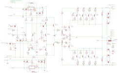
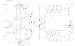
I do not see it. So, simplify. Is the bias spreader goofy? QSC used plain old diodes, so... try that. So the attached has diodes. If this does not pan out, simplify more.
That didn't help either.
I balanced out the power half and got the bias set before connecting it to the front end half, but no more luck than before, it's doing the same thing.
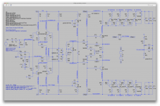
Now I've been putting together an idea as I mentioned earlier, to make use of dual complementary ltp topo, which is fully symmetric (attached 2nd screenshot).
It took a while and it is biasing and centering, with a little help from an extra offset adjustment on the negative input.
However the adjustment isn't very much, as without it the imbalance was only a few volts on the rails, pushing it slightly up. The diff amp inputs were at about 2mV each, very close to each other.
There is no effect of adjusting the offset to the speaker output, obviously because no dc can make it there, but I adjusted the offset to balance out the rails to center.
This worked for the operating point, so it looks like it works better, however, it all goes south when doing a transient analysis...
Attachments
Making some progress with my last attempt at the symmetric topo.
I realized after posting the reason why it went south when doing the transient analysis. My mistake, for not remembering that this output stage topo inverts.
Easy fix, switch to the other side of the ltp and let it rip.
I changed a few values, and adjusted the bias and rails center, and we have a pulse. That is, **** loads of oscillations, but a pulse nonetheless.
Now I'll take a shot at adding some compensation, and we'll see how that goes...
And one more detail, this way this amp doesn't invert.
Attachments
crossing posts, haven't looked yet at yours, was putting this together:
I hacked a bit a the asc, wouldn't show this at this stage except that it does basically seem to work and could help other thread participants sooner rather than later
I highly recommend getting to a working .tran sims before anything else is tried in sim
didn't have pot symbol required, so I rewired, minimally reworked bias, ~ 125 mA per output Q
moved output Zobel to the output Q node
ditched the extra Ccomp in the 2nd diff mirror
the state of the conmpensation is very "shoot from the hip", "sprikle some caps" not at all recommended except as a place to start real compensation knowing that it can "work"
the output DC sensing/control uses split feedback R - the same R as the AC gain
and couldn't resist some redrawing
Attachments

Last edited:
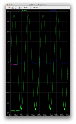
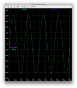
Here is my first attempt at compensation.
I managed to stop the oscillations, at least at the lowest frequencies. But some do show up again at 20khz, so more work is required to tweak the compensation.
This is very rough and it was just to make it work.
Actually the thd isn't too bad, especially with only 1v input and at 1khz.
I just used simple and basic miller and a global tiny cap.
The clipping is looking fairly nice, although I only tried it at 1khz, so far.
Attachments
-
 Screen Shot 2016-11-25 at 6.09.13 PM.png146.9 KB · Views: 66
 -
 Screen Shot 2016-11-25 at 6.06.25 PM.png144.2 KB · Views: 71
 -
 Screen Shot 2016-11-25 at 6.03.49 PM.png147 KB · Views: 76
 -
 Screen Shot 2016-11-25 at 6.01.31 PM.png145.8 KB · Views: 93
 -
 Screen Shot 2016-11-25 at 5.59.41 PM.png478.1 KB · Views: 130
 -
 Screen Shot 2016-11-25 at 5.55.43 PM.png142.6 KB · Views: 74
 -
 Screen Shot 2016-11-25 at 5.56.40 PM.png144 KB · Views: 69
Great thinking
We're hitting a wall here, so any fresh perspective is very welcome.
I looked at your schematic, and the key change seemed to me to be taking feedback from the split resistors to +-Vfloat. Makes sense, and I hope that is the breakthrough.
I pared away at my earlier design, and I will add the split feedback. I added a buffer on the Bias generator, hoping any interaction with the output stage would end. I did keep a mechanism for DC centering the outputs regardless of the input stage. It still is odd that this is failing but the previous generation of current feedback topology front ends worked well, and the new symmetric one is working. Soldier on.
Attachments
Simplify, simplify..
I see the symmetric amp works well. I puzzled why. I think it is not the symmetry, but the cancellation of input currents by the complementary differential amplifiers. The input offset current is an order of magnitude less. So I added an offset adjust in the attached, and also simplified further.
I see the symmetric amp works well. I puzzled why. I think it is not the symmetry, but the cancellation of input currents by the complementary differential amplifiers. The input offset current is an order of magnitude less. So I added an offset adjust in the attached, and also simplified further.
Attachments

Last edited:
Here is my first attempt at compensation.
I managed to stop the oscillations, at least at the lowest frequencies. But some do show up again at 20khz, so more work is required to tweak the compensation.
This is very rough and it was just to make it work.
Actually the thd isn't too bad, especially with only 1v input and at 1khz.
I just used simple and basic miller and a global tiny cap.
The clipping is looking fairly nice, although I only tried it at 1khz, so far.
This symmetric topology works better. I'm going forward with this one.
I switched to it in the attached schematic. I did a couple of things differently. I used zeners in the current source for better noise rejection. I use a 10k resistor to analog ground as part of the DC feedback divider, so the DC offset is multiplied 3x, but AC 33x.
Progress!
Attachments
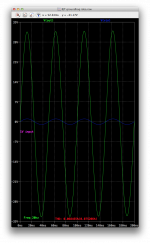
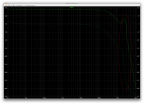
I've been trying to tweak the compensation and a few things to make it work better and try to get to a reasonable phase margin.
It's working rather well overall but I know it's not fully stable enough.
On a complex load, it would certainly have issues.
Anything higher than 4p7 on the global feedback will let oscillations come in.
Same thing with the miller caps, anything less than 270p will also let it oscillate.
I tried a few values for the degen resistors on the ltp, and what I have now seems to be the best I can find.
I adjusted down the output coil, and it may even be lowered some more, maybe, and the resistor in parallel seems best at that value as well.
Anywhere below 20khz, there are no signs of oscillation, but without those cap values, it will start oscillating at 20khz.
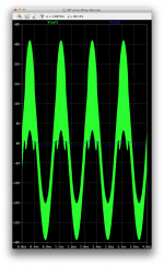
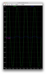
Look at the ac plot, where I highlighted the trouble area. I don't think we can get to a proper phase margin as is. The tweaks I tried did not make it right while keeping it running properly and with decent distortion.
Right now at 20khz, we have a little less than %0.05 thd, which isn't too bad for pa, but I think it could do better.
I did get it down around %0.02 but at the cost of other issues.
I'm posting the .asc sim file so someone more adept at compensation can attempt a better tweak than me.
There is one thing I did find out though, unrelated to the stability and compensation, which is that it was not such a good idea to move the tap of those 22ohms resistors from the drivers to the emitter of the O.Ds, because it causes a serious imbalance in bias current. With 3 pairs having the same current while the pair being tapped has in the order of 15% more than the rest.
It's working rather well overall but I know it's not fully stable enough.
On a complex load, it would certainly have issues.
Anything higher than 4p7 on the global feedback will let oscillations come in.
Same thing with the miller caps, anything less than 270p will also let it oscillate.
I tried a few values for the degen resistors on the ltp, and what I have now seems to be the best I can find.
I adjusted down the output coil, and it may even be lowered some more, maybe, and the resistor in parallel seems best at that value as well.
Anywhere below 20khz, there are no signs of oscillation, but without those cap values, it will start oscillating at 20khz.
Look at the ac plot, where I highlighted the trouble area. I don't think we can get to a proper phase margin as is. The tweaks I tried did not make it right while keeping it running properly and with decent distortion.
Right now at 20khz, we have a little less than %0.05 thd, which isn't too bad for pa, but I think it could do better.
I did get it down around %0.02 but at the cost of other issues.
I'm posting the .asc sim file so someone more adept at compensation can attempt a better tweak than me.
There is one thing I did find out though, unrelated to the stability and compensation, which is that it was not such a good idea to move the tap of those 22ohms resistors from the drivers to the emitter of the O.Ds, because it causes a serious imbalance in bias current. With 3 pairs having the same current while the pair being tapped has in the order of 15% more than the rest.
Attachments
This symmetric topology works better. I'm going forward with this one.
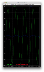
Yes, it does, and I have been making some progress with the one I was tweaking earlier, distortion down to 170ppm or so, and no more oscillations, but the phase margin isn't right at all, and all compensation schemes I tried haven't brought it to a reasonable amount so far. I had to really "sprinkle a few caps" here and there, looking to stop those pesky oscillations, and I found a compromise allowing for bandwidth and distortion but the phase margin hasn't been tamed yet.
I switched to it in the attached schematic. I did a couple of things differently. I used zeners in the current source for better noise rejection. I use a 10k resistor to analog ground as part of the DC feedback divider, so the DC offset is multiplied 3x, but AC 33x.
Ok, here it is attached, however it's not letting me adjust the bias at all.
I looked around for possible value mistakes and haven't found any so far. Maybe someone can point some out if any.
I was wondering about that 10k resistor (R9). Why is it attached there? Why not at the common of the 1 10ohms? This is causing a dissymmetry for sure. Was that intentional?
Progress!
Definitely! At least we know what works and what doesn't. And we did get a few that actually work fairly well, except for full stability and performance, for now.
Maybe we can arrive at something nice enough to be worth building.
I've been arbitrarily going for 60V rails, which seemed like a fair amount. With this, my attempt that worked puts out about 169W in 8ohms (resistive of course) before clipping starts, and no more than 0.05% thd at 20khz, before I tried tweaking the compensation.
I will post something later about this.
Attachments
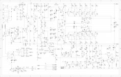
I find this schematic...
Cool! more stuff to try out.
But wow! Such a large part count and a boat load of diodes...
Cool! more stuff to try out.
But wow! Such a large part count and a boat load of diodes...
Without some counts...
Attachments
Last edited:
Spookydd said {my comments in brackets}:
"I've been trying to tweak the compensation... but I know it's not fully stable enough.
...
Anything higher than 4p7 on the global feedback will let oscillations come in.
This topology works. Fantastic. Now we need to get distortion down without losing stability. To that end, I made changes.
1. Increase differential pair emitter resistors to 100 ohm, decreasing gain but adding linearity.
2. Add current mirror on differential pair to increase gain and linearity
3. Increase current in differential pair to 6ma to increase slew rate and reduce noise.
4. Active current sources.
5. Made VAS a Szlikai pair, reducing loading on differential pair and increasing linearity and gain.
6. Small RC filter on input stage power.
7. Negative feedback on VAS to push up the open loop frequency rolloff.
8. lowered input filter low pass corner frequency.
These changes add complexity, but should greatly enhance performance and have negligible cost impact. Adding 14 small signal transistors costs about $0.42, compared to the $20 cost of the 8 output transistor, or to the $20 cost of the output filter caps, to the ~$50 power transformer.
I can easily lay out this simple board in less than a day if we use parts in my library, and know board shape to match our heat sink. Most of the layout time is setup and parts placement, not routing. So we need not worry about slightly increased complexity affecting board layout.
But we do need to validate that presumed benefit, so I do hope some of this can be simulated. Stability is primary, lower distortion secondary. Most of the changes are very well studied and accepted. One is less so. Does the negative feedback on the VAS really help, by pushing out the corner frequency above 20KHz?
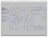
Attached is my current concept.
"I've been trying to tweak the compensation... but I know it's not fully stable enough.
...
Anything higher than 4p7 on the global feedback will let oscillations come in.
{Good to know, very sensitive to this value}
Same thing with the Miller caps, anything less than 270p will also let it oscillate.{Recall I said all the real amps like this I've seen had trouble with VAS oscillations, and both Symasym and the Hafler DH amps used a gross cap to ground in desperation. This is a little better as we get some benefit from the Miller feedback.}
I tried a few values for the degen resistors on the ltp, and what I have now seems to be the best I can find.{I went to 100 ohm, what did you use?}
I adjusted down the output coil, and it may even be lowered some more, maybe, and the resistor in parallel seems best at that value as well.{I used standard values, but always good to have a simulation to validate}
Anywhere below 20khz, there are no signs of oscillation, but without those cap values, it will start oscillating at 20khz.{the DH220 oscillated at 60 MHz when I removed that cap. Big issue to solve here}
Look at the ac plot, where I highlighted the trouble area. I don't think we can get to a proper phase margin as is. The tweaks I tried did not make it right while keeping it running properly and with decent distortion.{I'm using a 220k feedback resistor from VAS collector to base. According to D. Self, this reduces gain a little, but pushes the open loop rolloff from 800Hz to 20KHz, hope a simulation can validate that}
Right now at 20khz, we have a little less than %0.05 thd, which isn't too bad for pa, but I think it could do better."This topology works. Fantastic. Now we need to get distortion down without losing stability. To that end, I made changes.
1. Increase differential pair emitter resistors to 100 ohm, decreasing gain but adding linearity.
2. Add current mirror on differential pair to increase gain and linearity
3. Increase current in differential pair to 6ma to increase slew rate and reduce noise.
4. Active current sources.
5. Made VAS a Szlikai pair, reducing loading on differential pair and increasing linearity and gain.
6. Small RC filter on input stage power.
7. Negative feedback on VAS to push up the open loop frequency rolloff.
8. lowered input filter low pass corner frequency.
These changes add complexity, but should greatly enhance performance and have negligible cost impact. Adding 14 small signal transistors costs about $0.42, compared to the $20 cost of the 8 output transistor, or to the $20 cost of the output filter caps, to the ~$50 power transformer.
I can easily lay out this simple board in less than a day if we use parts in my library, and know board shape to match our heat sink. Most of the layout time is setup and parts placement, not routing. So we need not worry about slightly increased complexity affecting board layout.
But we do need to validate that presumed benefit, so I do hope some of this can be simulated. Stability is primary, lower distortion secondary. Most of the changes are very well studied and accepted. One is less so. Does the negative feedback on the VAS really help, by pushing out the corner frequency above 20KHz?
Attached is my current concept.
Attachments

Anything higher than 4p7 on the global feedback will let oscillations come in.{Good to know, very sensitive to this value}
Actually this wouldn't be the case for all amps of course. It was the case for that one in the topo used as it was.Same thing with the Miller caps, anything less than 270p will also let it oscillate.{Recall I said all the real amps like this I've seen had trouble with VAS oscillations, and both Symasym and the Hafler DH amps used a gross cap to ground in desperation. This is a little better as we get some benefit from the Miller feedback.}
I tried a few values for the degen resistors on the ltp, and what I have now seems to be the best I can find.{I went to 100 ohm, what did you use?}
I went down to 4.7 on the emitters at some point, but went back up to 10 later.
I adjusted down the output coil, and it may even be lowered some more, maybe, and the resistor in parallel seems best at that value as well.{I used standard values, but always good to have a simulation to validate}
{I'm using a 220k feedback resistor from VAS collector to base. According to D. Self, this reduces gain a little, but pushes the open loop rolloff from 800Hz to 20KHz, hope a simulation can validate that}
I'd be curious to experiment with that.
This topology works. Fantastic. Now we need to get distortion down without losing stability. To that end, I made changes.
I think so too, and this could end up being a good diy build.
2. Add current mirror on differential pair to increase gain and linearity
I was working on an other version of my "idea" with the symmetric ltp and didn't use mirrors, but I did replace the plain resistor dividers that power the tail of the ltps by current sources, and that caused a lot more issues, which I have yet to find proper compensation for with a decent phase margin. The resistive dividers worked better in that respect, with only plain and simple miller and global feedback based compensation.
Adding the current sources forced me to "sprinkle" some more caps here and there, and although I did get to stop the oscillations and got a compromise with fairly low distortion, the phase margin was all wrong, so not good yet.
3. Increase current in differential pair to 6ma to increase slew rate and reduce noise.
Ok on the slew rate, but how does this reduce noise? More current usually causes more noise doesn't it?
These changes add complexity, but should greatly enhance performance and have negligible cost impact.
Not a real big deal, as it's really not that much more.
But we do need to validate that presumed benefit, so I do hope some of this can be simulated.
Abso'freakin'lutely!
Stability is primary, lower distortion secondary.
True, as a very low distortion amp that oscillate ain't good for nothing...
Most of the changes are very well studied and accepted. One is less so.
Which is less so?
Does the negative feedback on the VAS really help, by pushing out the corner frequency above 20KHz?
Well, we'll find this out shortly won't we?
Attached is my current concept.
I'll get to work on this. It's again a good amount of changes, so it'll take some more time to redraw.
{my comments in brackets, my deletions as ...}
...I have been making some progress with the one I was tweaking earlier,... no more oscillations, but the phase margin isn't right at all... I had to really "sprinkle a few caps" here and there, ... but the phase margin hasn't been tamed yet.
{that worries me, we have to tame it}
{your design is} ... not letting me adjust the bias at all.
I looked around for possible value mistakes and haven't found any so far. Maybe someone can point some out if any.
{huh? The Vbe multiplier stuck? Could that be due to the balance network on the output, with diodes etc, overwhelming it? Well, OK, I took out the diodes and made the load 1.2k each side to ground in the attached schematic}
I was wondering about that 10k resistor (R9). Why is it attached there? Why not at the common of the 1 10ohms? This is causing a dissymmetry for sure. Was that intentional?
{Good catch. R9 was an editing mistake, already fixed already in next schematic posted. It was on the NFB midpoint and I moved things around and did not clean up the original area, I think. Whatever. It gives DC gain of 3x, leaving AC gain at 33x approximately}
...we know what works and what doesn't. And we did get a few that actually work fairly well, except for full stability and performance, for now. Maybe we can arrive at something nice enough to be worth building.
{totally agree}
I've been arbitrarily going for 60V rails, ...
{fine with me. Don't go much above 70v, or we'll have to cascode outputs or use MOSFETs. Second breakdown concerns me already, I don't know how QSC runs 93v}
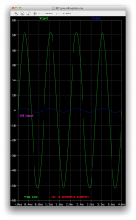
I looked at your Bode plots. Great! Nice job. That notch 2 MHz is weird. What's causing that? Or rather, how can we get rid of it?
I added 10 small signal transistors to my latest front end, each after careful thought. I did not add stages, just gain to existing stages, or local negative feedback. Each added stage adds phase shift, and the power types are the worst. I suggest simplifying the output section to a double, not a triple. Without the MJE340/350, we have more than enough drive from the VAS (Up to 75ma drive current to a transistor with a beta of 100+ which is current limited to 3A by the emitter resistor). Does that make sense?
I'm not sure how much of my latest schematic you will simulate. Of greatest interest to me is the effect of VAS negative feedback. I'd also like to see the effect on stability of reducing the output from triple to double. My other changes are known to work well, so not of as much concern.
What do you think?
In the attached schematic, the only change is the divider network to the output stage, to higher impedance load for the VAS. Hopefully that gets the Vbe multiplier to adjust.
Attachments
[/INDENT]....{large 270 pf Miller cap}... won't be applicable to anything else.
{I know, yet I have seen 330 pf to ground used here in two well regarded similar designs. Indicates a repetitive problem, crudely solved, and solved that way}
[/INDENT]I went about that high as well, but found no real benefit without actually causing some issues, especially with the various compromises to earn some decent phase margin.
I went down to 4.7 on the emitters at some point, but went back up to 10 later.
{I went with Self's suggestion of around 100 ohm. Trade lower gain for higher linearity, get the gain back using higher tail current and mirrors. I like the idea of being tolerant of badly matched pairs. What issues, spurious oscillations, under what conditions?}
....
I'd be curious to experiment with that. {the 220k feedback resistor from VAS collector to base. Yes, is Self on to something here? Been meaning to try it, we can always not stuff the resistor if it is useless.}
....
I was working on an other version of my "idea" with the symmetric ltp and didn't use mirrors, but I did replace the plain resistor dividers that power the tail of the ltps by current sources, and that caused a lot more issues, which I have yet to find proper compensation for with a decent phase margin. The resistive dividers worked better in that respect, with only plain and simple miller and global feedback based compensation.
Adding the current sources forced me to "sprinkle" some more caps here and there, and although I did get to stop the oscillations and got a compromise with fairly low distortion, the phase margin was all wrong, so not good yet.
{A priori, I don't like to sprinkle caps everywhere. That's what really bad bad digital designers did to hide glitches, and it always bit them in the end. I need to know the why before doing something. Anyway, I put the current sources in to give me a clean 6ma tail current to charge the Miller cap, and can always bypass with just 2.5k to the +-15v to compare}
....
....
....
....
I'll get to work on this. It's again a good amount of changes, so it'll take some more time to redraw.
Changes are always messy. I hope we can zero in and freeze it.
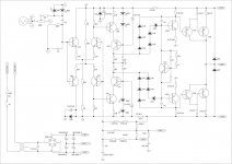
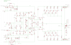
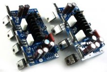
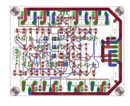
Have you thought about heatsinking, packaging and the like? It bears on board layout, which I am already thinking about. If we put 8 outputs on one side, it's long and thin. Say 2x5 ish. Let's you mount the board at right angles to the HS. Fits most situations. First photo below shows a bizarre layout with 8 outputs, mounted 4 per side of the board. An actual production board, odd layout. The alternative is an even longer board for all that stuff.
If we put 4 on opposite sides, they can bend down or mount co planar with the board, depending on heat sink. This is good for big plates like inside a sub, or long channel heat sinks, say. A trial layout in picture 2 of something else, 8 outputs.
Attachments
- Status
- Not open for further replies.
- Home
- Amplifiers
- Solid State
- grounded collector amp