With so many nice SiC devices becoming available, I thought it made a lot of sense to do a quasi complementary Firstwatt F4, I've modeled it with double die lateral mosfets but it should perform as well if not better with SiC devices.
Bias is 1.35A
I was too lazy to do a detailed bias circuit. I can do one if someone needs help with it.
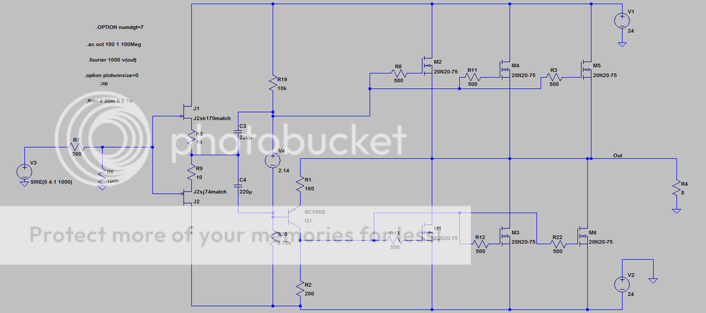
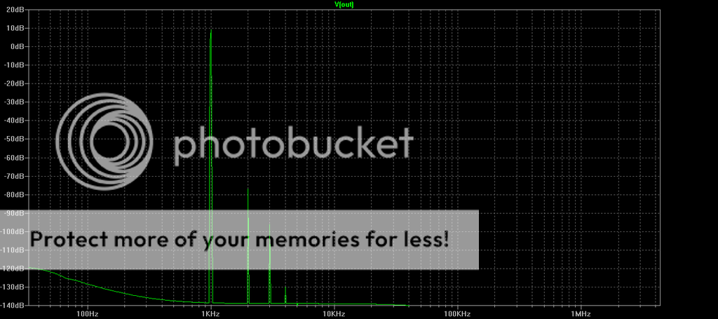
4Vpk into 8 Ohms
Total Harmonic Distortion: 0.005069%(0.005069%)
Bias is 1.35A
I was too lazy to do a detailed bias circuit. I can do one if someone needs help with it.
4Vpk into 8 Ohms
Total Harmonic Distortion: 0.005069%(0.005069%)
What are you thinking for psu voltage and estimated power output? Might be an interesting project!!
What are you thinking for psu voltage and estimated power output? Might be an interesting project!!
Anything between 23V and 34V (lets keep the capacitors no greater than 35v) would be ok, although I'd need to cascode the jfet buffer for anything over 26V.
So anything between 25W and 60W. If you wanted more power then best to go the balanced route which would get you over 200W if you were using 34V rails.
Last edited:
well, biasing scheme (both voltage/swing and temperature stability) is going to be most critical part of stage
besides that , dunno how it's gonna be better than regular complementary stage
as always , curiosity is perfect way to kill a cat , so I'm following your adventures
besides that , dunno how it's gonna be better than regular complementary stage
as always , curiosity is perfect way to kill a cat , so I'm following your adventures
Initial impressions were it simulates better than stock irfp240/9240 espescially when the bias is exceeded into low impedance.
I'll do some comparisons.
It's mostly about having more options. Eg No P Channel SiC parts etc
I'll do some comparisons.
It's mostly about having more options. Eg No P Channel SiC parts etc
Last edited:
well, biasing scheme (both voltage/swing and temperature stability) is going to be most critical part of stage
I have a few ideas and other variations of this circuit. I will throw out every idea I can think of on the table, and I'm sure you could improve on them or suggest some great ideas (I'm just a lego builder, some issues aren't always immediately obvious).
I'll stick to this basic idea first just get a feel for it's potential and compare circuits.
Papa please feel free to suggest some changes if required. I'll make full use of my limited brain cells first.
Thanks for reminding me about that one, brother Pat. I'll read over it again.
I'll let them go head to head for a showdown.
I'll let them go head to head for a showdown.
I would prefer the SRCFPP Power source follower Amplifier over the Taylor source follower.
It seems more simple and has a better PSRR.
SRCFPP Power Amplifiers
Cheers,
Johannes
It seems more simple and has a better PSRR.
SRCFPP Power Amplifiers
Cheers,
Johannes
I would prefer the SRCFPP Power source follower Amplifier over the Taylor source follower.
It seems more simple and has a better PSRR.
Cheers,
Johannes
How to DC couple ?
Patrick
Ok tested Taylor Source Follower.
Result: quasi above is a little better. Taylor is certainly not out of the race though it's a close second.
Result: quasi above is a little better. Taylor is certainly not out of the race though it's a close second.
Last edited:
You can adjust the resistor values to cancel out even order harmonics.
Patrick
I played around with the values to get the sought of distortion I am interested in at 4Vpk into 8 Ohms then I compared what happens to both circuits at 14V into 4 Ohms, to see how bad the crossover distortion is (if that is an accurate description) in both circuits.
I spent quite a bit of time optimising the circuit.
It's a very good circuit.
Last edited:


I took the liberty of jumping into this thread with the inverted SRPP or MU-Follower source follower.
This is a simple simulation with 14 volts (P-P) into a 4 ohm resistive load. Real life results will of course differ quite a bit due to reactive loads, resistance in cables, PCB-tracks etc.
I used some nice IXYS devices since I have not succeeded in adding the Cree SiC fets to LTSpice library.
I use a lot more current then I believe you do in your simulations. Even if it is possible to get very low levels of simulated THD with less current, I know from experience that most simple mosfet amps sound much better with some rich current heating the heatsinks and the listening room.
I hope you don't mind me adding some simulations. I am following this thread with great interest, since I have been exploring some different source follower amps lately, and this is where I ended up in my ruminations on the subject.
Cheers,
Johannes
I don't mind at all.
Try this model
.model 20N20-75 VDMOS (Rg=30 Vto={0.155-1.6m*50} Rs={0.12*(1+2.5m*50)} Kp={2.40/(1+7.4m*50)} Ksubthres={0.09*(1+1m*50)} Mtriode=0.3 Rd=0.16 Lambda=3m Cgdmax=200p Cgdmin=10p a=0.25 Cgs=1200p Cjo=2200p m=0.7 VJ=2.5 IS=8.0E-6 N=2.4 mfg=IH151206)
Then add 3 pairs to your output stage, bias at 1.35A and test at 14Vpk (ie 28V pk to pk) into 4 Ohms, I want to see how the circuit reacts when the bias is exceeded.
Just so I have something that I can compare with.
I agree with the more bias principle but for consistency to compare with what I have done so far it would be more meaningful to me if you test it like that,
It does not look that impressive. Lots of distortion. It is near clipping, which is obvious by the rich content of higher order harmonics. I am sorry for the ugly hack. I don't want to re-draw the whole amp, so I just shoehorned the extra devices into the existing simulation.

Cheers,
Johannes
Cheers,
Johannes

Here is the same amp with IXYS devices. The distortion drops markedly compared to the lateral devices. I see that the current increased to 1450 mA instead of 1350 mA. I increased the current slightly through the sensing fet in the MU current source.
Cheers,
Johannes
It does not look that impressive. Lots of distortion. It is near clipping, which is obvious by the rich content of higher order harmonics.
Cheers,
Johannes
That is not super terrible for that test. The quasi circuit does a bit better though.
To get the good result with the quasi circuit, resistors between source and drain at output need to be omitted, so it will be a lot easier making it work with devices with near zero temp coefficient hence the use of Laterals or you could use Infineon SiC or Semisouth R100. The other option would be to use a single Hockey Puck/sot227 with quite a bit of transconductance in which case the temperature coefficient is not as critical.
To be fair on your circuit though could you test it at 4Vpk into 8 Ohms. I'm interested in the degree of change in distortion not necessarily just the absolute value.
I'm not trying to achieve absolute low levels at 1W, but rather achieve a certain sound.
Last edited:
Round 1
Complementary vs Quasi Power Buffer Circuit using EXICON TO264
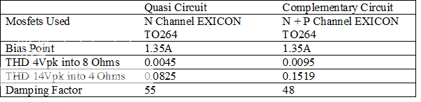
I can get even better results than this on the Quasi circuit but 2nd Harmonic cancellation is not my cup of tea.
Why I like the quasi circuit.
1) Easily obtain a dominant 2nd Harmonic
2) Distortion easily tunable (by addition or cancellation of 2nd Harmonic)
3) Access to a variety of far more interesting mosfets that don't have complementary P Channel parts, eg SiC Jfets etc
4) Cost savings (buying in larger quantities generaly means cheaper pricing)
5) The table of results speak for them self (certainly not inferior)
The only reason not to like this circuit is if you prefer 100% cancellation of 2nd Harmonic.
Complementary vs Quasi Power Buffer Circuit using EXICON TO264
I can get even better results than this on the Quasi circuit but 2nd Harmonic cancellation is not my cup of tea.
Why I like the quasi circuit.
1) Easily obtain a dominant 2nd Harmonic
2) Distortion easily tunable (by addition or cancellation of 2nd Harmonic)
3) Access to a variety of far more interesting mosfets that don't have complementary P Channel parts, eg SiC Jfets etc
4) Cost savings (buying in larger quantities generaly means cheaper pricing)
5) The table of results speak for them self (certainly not inferior)
The only reason not to like this circuit is if you prefer 100% cancellation of 2nd Harmonic.
Last edited:
- Status
- Not open for further replies.
- Home
- Amplifiers
- Pass Labs
- Quasi Complementary F4 (inspired by SiC)