HI there, what do u think about this idea, is it worth ? 😛
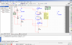
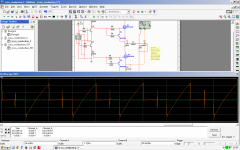
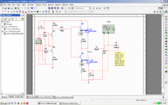
3rd and 4th pictures are for comparing with totem pole and complementary pair.
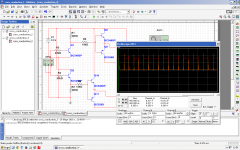
another question: is little rounding @ the square equal to better quality signal ?
this is possible with higher value of gate stopper.
I know its more heat but if is connected to quality ;d
will become class BD or AD because here are no crossover distort ;d
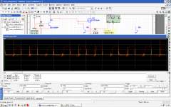
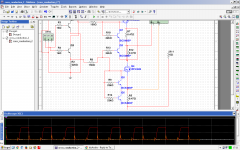
P.S. Anotherr question -> is this peak at 4th picture dangerous ? its only in the beginning and its short but.. dont know actually im afraid and concerned. I like the idea how both gate capacitanes kills each other. Charging, discharging itselfs.
3rd and 4th pictures are for comparing with totem pole and complementary pair.
another question: is little rounding @ the square equal to better quality signal ?
this is possible with higher value of gate stopper.
I know its more heat but if is connected to quality ;d
will become class BD or AD because here are no crossover distort ;d
P.S. Anotherr question -> is this peak at 4th picture dangerous ? its only in the beginning and its short but.. dont know actually im afraid and concerned. I like the idea how both gate capacitanes kills each other. Charging, discharging itselfs.
Attachments
Last edited:
i have new idea like the protection in normal amplifiers.
note that the down side is disconnected. its because it works better without it.
P.S. i have made a mistake in down side, thats why it works worse
my only concern is that the amplitude is not 12v but 7.6v
P.S. 2 -> Corrected the error and works but its the better with one side only because its same
note that the down side is disconnected. its because it works better without it.
P.S. i have made a mistake in down side, thats why it works worse
my only concern is that the amplitude is not 12v but 7.6v
P.S. 2 -> Corrected the error and works but its the better with one side only because its same
Attachments
Last edited:
Nobody answers, because your approach basically dont reflect any practical reason, and your sentences are hard to understand, and your simulation results dont show details.
The current state of art reached about 1 ns of effective dead time at 50-100V and 10A, while your new idea shows about 1 us. If your goal is to actually build some good amp, then use integrated solutions, or other proven concept.
If you want to understand how different parameters affect sound quality, then you can simulate ideal circuits with controlled nonidealities. For example ideal switches paralleled by diodes with dead time introduced in the control signal. To see what it really cause you have to simulate more than 1 period of audio signal (for example 3 ms for 500 Hz), with significant time resolution (for example 10 ns if you want to see the effect of 100 ns of dead time).
When you know what dead time causes and understand how, then you can start optimising switching process, by more deeply analysing the switching waveforms and experimenting with different gate drives, etc...
The 4th picture shows not switch mode gate drive. It is dissipative, unless you overdrive it. About 10 V higher input signal is needed to be really ClassD. But otherwise it would be very good.
Thanks for the answer, my idea is to stop cross conduction without deadtime use, i know its possible 🙂 Greetings.
i already made class d amp and it sounds very good but im using ir2111 with big dead time, i dont want to use any. (even with the big deadtime my sch sounds like class A :O )
you said the 4th is good but is this peak at the current in the beginning bad ?
my logic is to discharge the gate capacitance when there is a current flow at the output (sensed via 0.22 resistors) and when both gates are 1.
now im thinking that theres no need of current sensing, only two transistors for discharging controlled by the gates.
Last edited:
this works, 100mv max / 0.47 ohm = 200ma MAX throught both fets
WITH NO DEAD TIME !
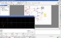
P.S. added 2nd picture, BETTER one, same but need less base current and less collector current for the dischargers 🙂
WITH NO DEAD TIME !
P.S. added 2nd picture, BETTER one, same but need less base current and less collector current for the dischargers 🙂
Attachments

Last edited:
Good to see some new ideas, it's how we progress despite the luddites 😉
Have you considered using a simple (ferrite or air) transformer as a way to get minimum dead time and avoid shoot-through in mosfets?
With a transformer you can effectively run it like a tube push-pull but with class-D pulses. Then you just filter the secondary as usual.
It has disadvantages but it would allow zero dead time as shoot-through would not be an issue. I'm not sure it would be fast enough with ferrite though, but it's another thing to look into and simple in concept.
...there is again the topic how to define dead time..
The time while both gate drive outputs of a half bridge driver are low?
Or the time while both Vgs are below their gate plateau voltage?
Obviously the first does not apply here, because there is no such half bridge driver IC.
If you apply the second definition and start looking into short dead times or overlap situations, you will notice that the wording of dead time is misleading.
In fact both switches are performing an analog transition between low impedance and high impedance. When going to short dead times this transition is likely to become longer than the adjusted 'dead time'. At this point or when going for controlled overlap, the wording of dead time really does not make sense any more. Instead one has to examine the change of impedances and resulting currents & voltages during the few nanoseconds of transition. Besides the resistive change of impedance you will also have to take into account the heavily non linear capacitive impedances of the switches, including Qrr behavior and the inductor current.
Overall you will find a dilemma between achiving ZVS during idle, which is asking for a certain 'dead time' and on the other hand going for zero 'dead time' or even overlap which is helpful for low distortion (and reducing Qrr issues at high loads if your MosFets provide low enough Rdson).
In order to get a valid picture of your switching method you always should examine both transitions (Hi2Low & Low2Hi) at idle, at most positive and at most negative current.
In any case the MosFets do not care how you generate your gate drive timings. They just act according to the timings and drive impedances with which you feed them. So you are of course free to consider an event driven BJT timing machine instead of ns counters or delay gates or half bridge drivers or any other method.
Well, as Pafi already mentioned: In the last shown solution the upper MosFet is not fully switched on, but more operated as a source follower. When high positive load currents have to be delivered Vds will not get close to zero and the device will show undesired conduction losses. Furtheron the output voltage of the half bridge during Hi-state will strongly depend on the load current and this translates into distortion. So you really should spend a gate drive, which can lift the gate higher than the drain.
P.S:
Don't forget that component parameters will vary with temperature, which becomes of specific importance when your circuit relies on the storage times of BJTs which are driven with high impedances.
I tried this real life (mentioned in post #6) and it works better than ir2111, square wave is not rounded at all, and the sound is awsome.
with ir2111 square is little rounded,
with irf530+9530 the result is not very good. (not beautyful squarewave)
only problem i cant figure out is that my amp is very quiet.
im running it with single supply 12v, but this is not the problem since its quiter than a tda2003.
the duty cycle goes min and max very good, this is not the problem.
the mosfets gates are 0-12V -> good low Rds
Is it possible to be the filter?
Iam seening 100khz at the out and its larger than the signal.
I am using 1uF decoupling, 100uH and 47n to ground because i have only these values.
I have another inductor but dont know its value.
(little offtopic) 😕
Attachments
Yes!
I solved the problem !
Everything works fine now.
It was the 1uf decoupling cap.
It was before the LPF.
I removed it and added 2200uF instead.(this time after the filter).
Doesn't make sense to me but it didn't worked with it before the LPF ??
There is 100khz PWM and the 1uF corner freq is 27kHz. 😕
Its great its working not quiet. Im very glad. 🙄
Attachments
This idea ROCKS,
This idea FOR THE WIN,
cross_conduction_quasi,
class D quasi,
quasi and class D D:,
class AD, class BD, class ABD,
ROCKS !😀
MY AMP SOUNDS FANTASTIC, WILL OPEN THREAD SOON TO SHOW IT, VERY VERY GOOD.
This idea FOR THE WIN,
cross_conduction_quasi,
class D quasi,
quasi and class D D:,
class AD, class BD, class ABD,
ROCKS !😀
MY AMP SOUNDS FANTASTIC, WILL OPEN THREAD SOON TO SHOW IT, VERY VERY GOOD.
Attachments
Last edited:
This idea ROCKS,
This idea FOR THE WIN,
cross_conduction_quasi,
class D quasi,
quasi and class D D:,
class AD, class BD, class ABD,
ROCKS !😀
MY AMP SOUNDS FANTASTIC, WILL OPEN THREAD SOON TO SHOW IT, VERY VERY GOOD.
Very good! Seeing your last picture you invented a quasy-complementary ClassB (or C) power stage! You are so very proud for good reason.
Are you advertising something? Else why do you overload your post with keywords?
Last edited:
Very good! Seeing your last picture you invented a quasy-complementary ClassB (or C) power stage! You are so very proud for good reason.
Are you advertising something? Else why do you overload your post with keywords?
thats where my idea comes from.im not reinvented it.
i inveted its use in class d and theres no cross conduction ?
Also transtors have more less capacitace.
because i can'ted decide which to use, i wanted to use all of them, why not ?
P.s. My amp works good, but why when i plug it with 36V instead 12, there no difference ?
only heat in the fets ? why they're heating and quiet as 12v supply ?
Last edited:
My amp works good, but why when i plug it with 36V instead 12, there no difference ?
only heat in the fets ?
Because it is still Class B, not Class D. Higher input signal is needed for higher output. It is linear/dissipative. The same issue as I mentioned in connection with the 4th picture of 1st post.
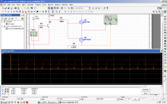
no, input is maxed, i already mentioned that duty cycle goes very minimum and very maximum. higher inp signal results clipping and distort.
its not linear since both fets get 0-12V square pulses, not rounded, very square.
with 12v supply and no heat at all (i am not using heatsink).
this is not with the quasi, i havent tried it yet.
this is with the cross(X) discharging sch.
its not linear since both fets get 0-12V square pulses, not rounded, very square.
with 12v supply and no heat at all (i am not using heatsink).
this is not with the quasi, i havent tried it yet.
this is with the cross(X) discharging sch.
Yes, referenced to GND. And this is clearly not enough for driving high side FET. Do you know what a high side driver does? Gate to source voltage should be 12 V, not Gate to GND! The way you connected the transistors, at high voltage you can get only damaged parts, not amplifier.0-12V
Since no amp is shown, only power stage, obviously I talk about its input (=PWM signal), not the audio signal.no, input is maxed, i already mentioned that duty cycle goes very minimum and very maximum. higher inp signal results clipping and distort.
Yes, you are right.Yes, referenced to GND. And this is clearly not enough for driving high side FET. Do you know what a high side driver does? Gate to source voltage should be 12 V, not Gate to GND! The way you connected the transistors, at high voltage you can get only damaged parts, not amplifier.
I didnt understand that.Since no amp is shown, only power stage, obviously I talk about its input (=PWM signal), not the audio signal.
P.S. Now i understand you talked about voltage not duty cycle or audio signal.
Is there any mosfet driver with 1 input, low dead time for audio, DIP package and 8 pins ?
What i know for low dead time is with 2 inputs and many pins.
Thanks.
What i know for low dead time is with 2 inputs and many pins.
Thanks.
now im suffering crappy soundcard.
its ok qualityfull but this noise 🙁
my laptop's one is dead from breadboard playing.
very very noisy 1$ usb soundcard.
its impossible to listen music throught it.
i kill the noise with series resistor to audio signal but this means quiet.
--------
I attached HF transformer (from ATX supply) at the output before LPF and it works but ->
question: It kills low frequency. Why ?
I am putting 100khz to the transformer not hertzes.
Last edited:
...I attached HF transformer (from ATX supply) at the output before LPF and it works but ->
question: It kills low frequency. Why ?
I am putting 100khz to the transformer not hertzes.
Because low frequency is low frequency. 🙂 PWM contains exactly the same spectrum as the modulating audio signal, plus other components at high freq. Transmitting only high freq gives the result you experienced.
"At the output" OF WHAT?
Lazyness is good only if it comes together with knowledge...
- Status
- Not open for further replies.
- Home
- Amplifiers
- Class D
- cross conduction idea