Mosfet54,
Your updated schematic looks better. You might even be able to adjust the other resistor values to eliminate R10 and R2 entirely if you wanted. Be sure that the Vbe multiplier transistor is in thermal contact with the heatsink so that it works properly.
I'm not sure if BS170 is a good choice or not. They are rated to a max of 60V and your total system voltage is 74V, so I don't know if that could cause problems. I'm fairly inexperienced compared to some here, so maybe someone else can comment on that? 😛
I do not believe that using a long-tailed pair would not necessarily increase the sound quality over an op-amp, but using higher voltage transistors would just make it easier to design for the +/- 37V supply without having to find a high voltage rated op-amp to use here. Either way, the negative feedback of the system is what helps to keep the distortion fairly low.
I'm not sure what you mean by adding another low power stage in between the op amp and the power stage. My design from before used a class A stage between the long-tailed pair and the power stage, and the class A stage also served as part of the biasing network for the power stage. The bias of the class A stage was pretty much set by the long-tailed pair and controlled by the feedback of the overall system. Whether you want to implement it this way or not is your choice. I'm sure there are other ways of accomplishing this, especially in a way that will be more symmetrical around your bipolar supply rather than the single supply I used in my design.
When testing this, be sure to keep an eye out for oscillations. be sure to use some form of current limiting as discussed above, and consider connecting an ammeter in line with the power lines to set the bias current properly and to make sure the current draw of the system is what you are expecting. Maintaining a tidy physical layout will be very important to prevent oscillation (also, just for looks, consider cleaning the excess flux off your boards using some rubbing alchohol after you solder them 😉). Start up the circuit with the biasing current turned all the way down and slowly turn it up. Hopefully most of this should be fairly common sense, but it never hurts to be careful, especially if you are worried about losing another pair of power transistors.
Last edited:
under "low power stage" i meant 1 or 2 transistors which amp. the voltage from the opamp. ex. op amp output +-15v ; low power stage output +-20-30v ( i do not know max gate voltages )
and this i think is better sound quality than long tailed pair using full +-37 voltage 🙂
heheh nothing compares class D half-bridge feeded with 74v 😀
im gonna test this because i invented how to stop fets conducting two at a time in my class D design; totem pole drive didn't help.
there was 5.8v in the cross point where two of them conducting @5.8v
=> if not use full 0-12v range but 0-6v - these 5.8 gonna turn 2.9 and this will help because at 2.9 is very small chance of conduction 🙂
=> 74v half bridge = +-37 output voltage which is woow ;gonna blow speakers I THINK 😀
aaand 37^2 / 6 ohm = 1369(fatal 69) / 6 = 228w real max power
IM SO EXCITED AND PLEASED, i CANT SLEEP 😡@
MOSFET SOUND IS VERY GOOD, i do not know if this is because i know they sound like valves, tubes 😀
i never designed transistor amp to compare, i have one sony commercial amp and studio2 old bulgarian with 2n3055
and i do not believe commercials enought to compare my own child 😀 🙂
Last edited:
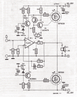
abetir, what is this schematic dude 😀
jilny, R10 and R2 are for protection if one end of the supply gone and there are only one and ground 😀
p.s. ooh this was long before i start to use decoupling cap at the output 😀
p.s.2 Is it good idea to connect them to output (sorces) instead of ground (lowering input impedance of the fets)
ofc is best with smaller count of parts and i dont like them but i think they are good to output instead ground for lowering input impedance of the fets
Last edited:
this is amazing, with just 20ma standby, 0.001% THD
im plan to use 100ma which is 74*0.1 = 7.4 W
too good enough for 0.00000000000 % distort
need to install LTspice and test there 😛
or i would calculate it if it linear function standby current and distortion
gona take two samples and gona take k (y=x*k) and gonna calculate distortion below 0.000% 😀
after this will check in LTspice and compare my calculations 😀
Last edited:
hehe it looks like IC now 😀 😀 😀 
i cant believe this is happening
how to parallel fets ? i know its dangerous !! with 0.22 ohm source resistors or only with gate stoppers ?
i cant believe this is happening
how to parallel fets ? i know its dangerous !! with 0.22 ohm source resistors or only with gate stoppers ?
Attachments
Last edited:
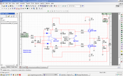
Easy one first 🙂 The bulb tester normally goes in the mains supply, so in series with the primary of the transformer.
Nearly there with the circuit... just a couple of errors.
1/ C2 and C3 are preventing the opamp from exerting any DC control over the FET's.
2/ Your feedback take off point is incorrect.
3/ Using a FET for the multipler can be very successful but I wouldn't go down that route here. Whatever you use has no effect on the sound quality as such.
Look how the multiplier is shunted by a largish cap. Note the feedback point and that the opamp is directly coupled to the FET's. Because the opamp is connected to the lower end of the multiplier, the lower 10k (22k in yours) isn't needed.
The bulb tester normally goes in the mains supply, so in series with the primary of the transformer.
I know this. Thanks.
1/ C2 and C3 are preventing the opamp from exerting any DC control over the FET's.
This means it works but with distort ?
In multisim this variant is better than resistored one :O
THis gonna solve like shunting C2 and 3 with resistors 😀 (both methods) xD
2/ Your feedback take off point is incorrect.
Again in multisim this variant is better.
And whats the point to be before the cap ?
I think its the fets need to touch the ground via the feedback to allow conduction. And I added this 2k before the cap just for this if my feedback is after the cap for better quality. ??????? 😕
Look how the multiplier is shunted by a largish cap.
Thanks. I was confused about the value of this cap and didnt used at all 😀 😎 cool
Buuut, I think I doesnt have 100u right now, What to use instead ? Smaller or bigger ?
Because the opamp is connected to the lower end of the multiplier, the lower 10k (22k in yours) isn't needed.
This is class AB I think and mine is B for little heat 😀
That think:
1/ C2 and C3 are preventing the opamp from exerting any DC control over the FET's.
I solve not with AB, but just with injecting the signal between two resistors.
they are going to both gates and this is class B 🙂
----------
Heey my parts are here, gonna do some soldering 😎
Heey my circuit looks like a soap
 😀 😎
😀 😎 
Last edited:
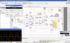
Although it works in simulation with your feedback connection, it won't work in practice. This is because the opamp in simulation is 'perfect' and it has no imbalances or offset errors.
You can see that here where I have broken the feedback connection. The opamp inputs show as zero volts (femto volts) and so does the output. Theoretically perfect, in practice the opamp output will swing hard to one of the rails.

You can see that here where I have broken the feedback connection. The opamp inputs show as zero volts (femto volts) and so does the output. Theoretically perfect, in practice the opamp output will swing hard to one of the rails.
I know this. Thanks.
Oh **** you said primary not secondary + or - 😀
That would be dangerous 😀
It was the feedback but why it differs from the simulation and such a big difference 😕 
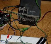
I am attaching photos 😉

And a problem: 50hz brum. Is this from power supply capacitors ?
They are 4700uf aand I short circuited them many times unexpectedly.. They are damaged or they are too small ?
I am attaching photos 😉
And a problem: 50hz brum. Is this from power supply capacitors ?
They are 4700uf aand I short circuited them many times unexpectedly.. They are damaged or they are too small ?
Attachments

Last edited:
Hey, Ive read somewhere that its good to bias the opamp in class A with 10k resistor from out to ground ??? 😕
Smb tested this ?
I tested but hear no difference 😀
Im gonna design my smps 33v single polar and design this schematic for single supply 🙂
Or try to make middle stage for all of the voltage but im afraid of this 50hz brum 😀
Door's window resonate from it in Idle state. When make fb as desired ..
Smb tested this ?
I tested but hear no difference 😀
Im gonna design my smps 33v single polar and design this schematic for single supply 🙂
Or try to make middle stage for all of the voltage but im afraid of this 50hz brum 😀
Door's window resonate from it in Idle state. When make fb as desired ..
Last edited:
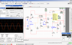
I am posting an UPdated circuit.
This schematic is awsome and works pretty good IN REAL LIFE 🙂
No heat at all.
This schematic is awsome and works pretty good IN REAL LIFE 🙂
No heat at all.
Attachments
Last edited:
And class AB little better i see 😱 🙄
THANK U ALL 🙂 I am thinking of using and the second opamp as inverter and use two same IRFs ex. two IRF540. Two N channels 🙂
Maybe low distort this way 😀
THANK U ALL 🙂 I am thinking of using and the second opamp as inverter and use two same IRFs ex. two IRF540. Two N channels 🙂
Maybe low distort this way 😀
Attachments
Last edited:
Oh **** you said primary not secondary + or - 😀
That would be dangerous 😀
Not if you wire it safely.
Hey, Ive read somewhere that its good to bias the opamp in class A with 10k resistor from out to ground
Don't believe everything you read.
It was the feedback but why it differs from the simulation and such a big difference....... And a problem: 50hz brum. Is this from power supply capacitors ?
They are 4700uf aand I short circuited them many times unexpectedly.. They are damaged or they are too small ?
This works and the simulation didn't simply, because the simulation doesn't account for the 'real world' characteristics of the opamp (as I demonstrated above).
And its a lot better with TL072 but using it overclocked @ 20 volts 😀 because Im too lazy a*s to change the zeners with 16v ones .. Whatever they are cheap.
This produce a lot of heat in up volumes and with tl072 is a little less i think.
It works very well with both of the op amps paralleled too.
ONLY NE5532 IS FOR LOW FREQ AMPS
This produce a lot of heat in up volumes and with tl072 is a little less i think.
It works very well with both of the op amps paralleled too.
ONLY NE5532 IS FOR LOW FREQ AMPS
- Status
- Not open for further replies.
- Home
- Amplifiers
- Solid State
- very good mosfet design failure