Ok, you could attach the input board to DAM with ribbon cables, although that is not optimal. Keep the cables as short as possible.
It will require a 26-pin (2x13) cable for DAM J3 connector. If you use standard female connectors on the input board, you will need a male-female terminated ribbon cable (as opposed to common female-female). Or, you could use male pinheaders on the input board. Note that the new input board will use SMD parts for this connector.
If you are building a dual DAM balanced setup, you will need two such cables.
There are only 2 wires actually needed from DAM J2 connector (PWR A+ and PWR +1.2), so I suggest to use "Dupont wires" for that. These only need to be connected to one DAM board, not to both.
Sorry if this is a stupid question but how would you connect two ribbon cables to one connector?
Sorry if this is a stupid question but how would you connect two ribbon cables to one connector?
Not stupid at all, it was rather tricky to come up with a clean solution that just clicks together. There will be two connectors - one on top, the other one on the bottom. That is the reason for using SMD connectors in this position.
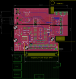
The input board layout is nearly done. Just need to verify a couple more things. If everything goes smoothly, I should have test prototypes ready by the end of next week.
Some notable updates:
Some notable updates:
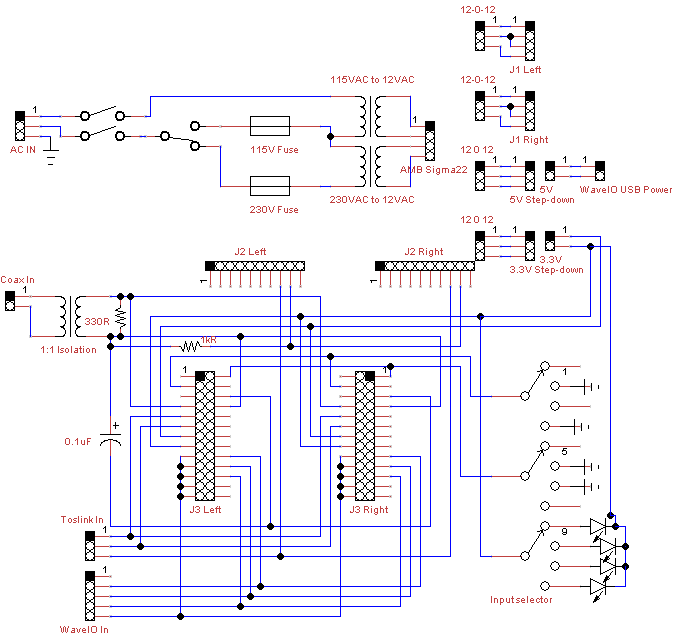
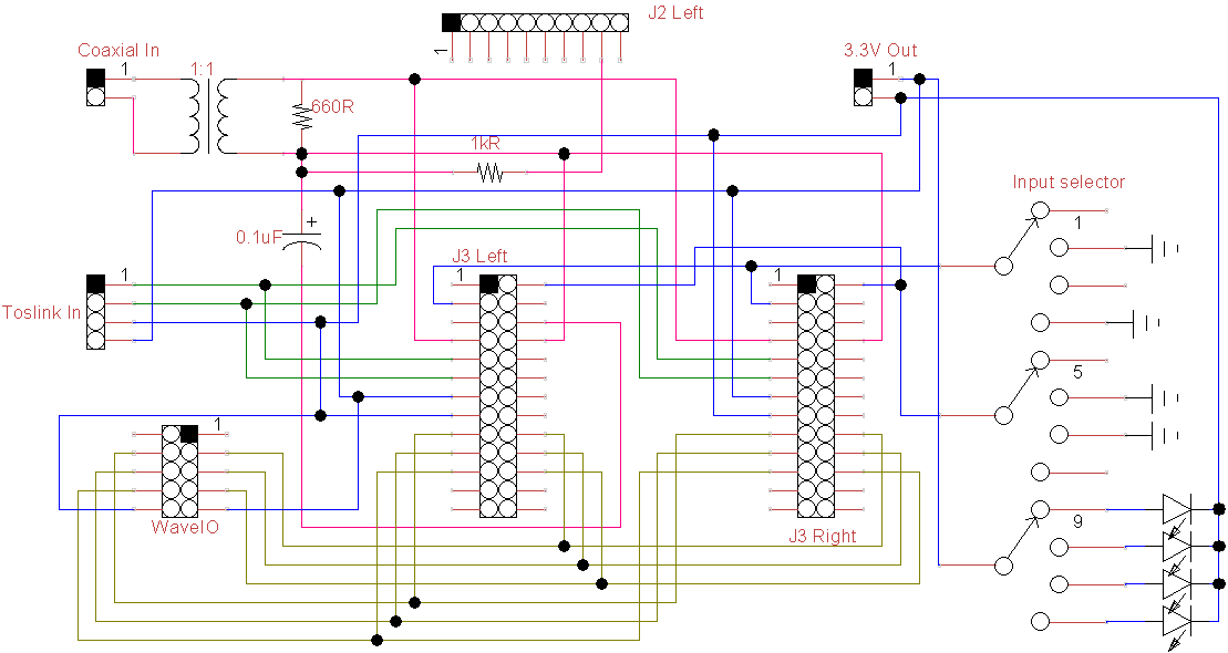
- Linear 5V/1A regulator added to supply power to Raspberry Pi and/or other 5V devices such as Arduino, BBB, WaveIO USB
- Needs a single unregulated 7-12VDC power supply to power all of the above.
- P-MOSFET ideal diode to protect from reversed power supply polarity.
- True balanced dual DAM1021 option. The second DAM can be plugged in on top of the input board. It will require mounting the DAM J3 connector on the bottom of DAM board.
- Dedicated optional connector for WaveIO USB interface. Should work, but it is untested since I don't own a WaveIO board.
- Current limiting resistors to protect DAM1021 output lines in case the connected microcontroller GPIO pins are accidentally programmed to output mode.
Attachments
Does one need 2 (or more?) muting modules if running a dual DAM balanced setup?
Only one module would be needed. The design is not finished yet, it will probably need to have a second relay installed for balanced setup.
I'm tempted to design an entire backplane board tbh.
If you prefer to go that route, there is a chinese guy who had designed a backplane type of board. Check the main DAM1021 thread, it's there somewhere.
I can't edit my post for some reason, but I forgot to say ask for suggestions for the step-down transformers for the 5V and 3.3V voltages.
Too late, I've already made this...
Any suggestions? 🙂
- You should not parallel the regulated DAM power supplies.
- J3 pins are mirrored for left and right channels???
- Consider the input impedance for the differential spdif input.
- It is better to have a GND wire for each I2S signal.
The 15-0-15VAC output will be passed through an AMB Sigma22 which will have 4 different 12-0-12VDCoutputs. Two will be used for the DAM supplies and 2 for the other voltages. Do you mean I should use a separate supply for each?You should not parallel the regulated DAM power supplies.
Yea, simple mistake of flipping it, already corrected.J3 pins are mirrored for left and right channels???
Sorry, I don't understand this. What difference does it make when put in differential mode?Consider the input impedance for the differential spdif input.
The WaveIO only has one ground port so how do I implement this?It is better to have a GND wire for each I2S signal.
I'm...actually somewhat new to this electronics thing, so sorry for any silly questions 😱
I am referring to power regulators located on the DAM itself.
Input impedance has nothing to do with switching dam in balanced mode, it is about connecting two inputs in parallel.
The waveio documentation I saw had a 10 pin connector for I2S signals, 5 pins of which were gnd lines.
Input impedance has nothing to do with switching dam in balanced mode, it is about connecting two inputs in parallel.
The waveio documentation I saw had a 10 pin connector for I2S signals, 5 pins of which were gnd lines.
Ahh, so each power line for 3.3V and 1.2V should be connected to only one DAM pin, right?I am referring to power regulators located on the DAM itself.
I THINK this means that I double the resistor value, right?Input impedance has nothing to do with switching dam in balanced mode, it is about connecting two inputs in parallel.
Oops, checked it again and there it is.The waveio documentation I saw had a 10 pin connector for I2S signals, 5 pins of which were gnd lines.
A new production run of updated DAM1021 hardware is expected to be available in August. I will confirm with Soeren if there are any relevant changes to connector layout, but I don't expect any compatibility issues.
Hi Normundss,
Did you get the confirmation from Soren that next revised boards would be compatible with your input boards ?
Thanx for the feedback.
Hi Normundss,
Did you get the confirmation from Soren that next revised boards would be compatible with your input boards ?
Thanx for the feedback.
Yes, he said the next batch will be physically the same. So all the V1 boards should still work with the new production DAM1021s for the features originally supported. The new V2 input boards will enable use of some of the new firmware functions, and provide lots of additional connectivity features as described in the first post of this thread.
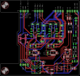
Muting board
Finally it looks like all issues have been worked out and the muting board design is finished. I just need to clean up some silkscreen labelings for the PCBs and within a couple of days they will be sent off for test board manufacturing. I will post detailed schematics and BOM once the test boards have been verified. If everything turns out good, the production boards should be ready for shipping in about a month.
The muting board stacks directly onto DAM1021 J7 header (the unbuffered outputs. It should even fit when the onboard XLR connectors are mounted, although I do not recommend using them.
Muting is done by shunting the outputs to ground with normally closed relay contacts. Since the pin18 muting control does not work properly as of the current firmware release, and it can be quite difficult to attach wiring directly to that pin, the mute control is implemented independently.
The power-on muting uses a delay circuit which turns on the outputs approximately 8 seconds after power is applied.
The power-off muting uses AC detection and will mute the outputs within approximately 30 ms after loss of AC power.
Optionally these timer based circuits can be bypassed and pin18 driven control can be implemented.
There are unpopulated footprints for implementing SE to balanced output buffers using THAT1646/DRV134 chips. The optional buffers use through hole parts for easier hand assembly. With a good power supply I believe they can provide better performance than the onboard buffers.
The board will optionally support true balanced configuration. An additional relay needs to be added to the board to mute the second DAC.
In true balanced setup output signal can be taken directly from the unbuffered outputs, or optional output buffers can be implemented using THAT1606 ICs. These chips are only available in smd version, so there is no through hole option possible here.
It should be possible to use the balanced unbuffered hardware setup for a 2-way crossover use in single ended mode, although I have not tried that.
Attachments
Finally it looks like all issues have been worked out and the muting board design is finished.
normundss, your fine work will help doing of soren's DAC a refined product.
Thanks again.
Laurent
- Home
- Group Buys
- Input and switch boards for Soekris DAM1021 DAC