What's even more confusing in the D's is in the gain/master slv table and diagram on p14 the resistors are R1 & R2, yet in the larger full schematic they are R11 & R12!... I know it wasn't necessarily intended for general public release. It is easy to figure out why so many of the boards around vary quite a bit....lol
I didn't connect any other component, so no worries 🙂Irribeo,
in the 3116 ds is a clear statement to me that there must be a cap for sure.
-.-
Yes datasheet has copied pasted parts of other datasheet LOLOL just like the 5.6k falls out of copy paste machine 🙂 Just like they forgot to copy paste the noise (creating?) filter on AVCC 🙂 They should really follow copy paste classes, we agree.
Signal to gatedrive is half the effective switchingfrequency I believe (BD), 400khz appearing on gvdd means it is very close to output?, I don't think putting 67khz there (now with Wima 1uF c15) can be helpfull, but board is in garage and I hardly go there🙂
just moving on... I have been looking at outputs.
I used ltspice to do the lc filter, to which I added the output circuit, including adding the bootstrap mod.
I did two versions, below is the lc filter with ouput circuit. Both versions with the 15uH coil and 470nF cap, and the bootstrap mod values as in the EVM datasheet.
One of the graphs show the rest of the output circuit as per datasheet values, the other with changed values I was playing with.
My question is.... which looks the better out the two? And why?
I havent named the graphs properly, and also not included the values, as to not highlight which circuit is which. To prevent any biased judgement from those using set values already.
I'd would go for "-ltspicewithoutputcircuit". It has some more roll-off, but deeper cut-off. 🙂
But i'm not sure if you'll hear it.
But i'm not sure if you'll hear it.
I'd would go for "-ltspicewithoutputcircuit". It has some more roll-off, but deeper cut-off. 🙂
But i'm not sure if you'll hear it.
Thanks for opinion. This isn't my values, but example to assess what a change in values I tried would show.
Thanks for opinion. This isn't my values, but example to assess what a change in values I tried would show.
The only difference in the two circuits is the two caps+resistor in the output circuit, the bootstrap mod and lc filter values the same in both.
The datasheet values show less peaking without bootstrap mod, yet more at +20khz beyond the lc cut off with bootstrap mod.
The changed values show more peaking without bootstrap, yet less at the lc cut off with bootstrap mod.
The trace shown on graph is the line just before entering final "speaker" resistor.
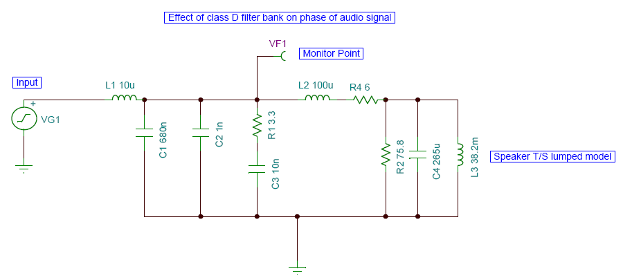
You can model the speaker T/S in spice as lumped RLC elements.
http://www.diyaudio.com/forums/class-d/237086-tpa3116d2-amp-448.html#post4029514
Here was my model of the LC filter and snubbers for a reactive speaker load:
http://www.diyaudio.com/forums/class-d/237086-tpa3116d2-amp-448.html#post4029514
Here was my model of the LC filter and snubbers for a reactive speaker load:
I think it is a nominal 8ohm. You can see the 6ohm Re value.
Gave it a try in spice, gave pretty much same result as putting series 350uh/8ohm combination as driver. Cheers though, as trying driver modelled as you showed above enabled me to figure the circuit properly with both channels, so it is exactly as on board. Not the SE version.
The examples I graphed previously showed one with datasheet output circuit values which pushed the filter freq up to 60k+, where as the graph which showed the 41k filter was same lc values with the output circuit values altered.
To be more specific, I divided the LC filter cap value by 11. Then split that figure in a 10:1 ratio, and used those figures in the output circuit which stayed as a 41k filter..
Now I can model the effect of changing output filter values, and ratios, optimising them specifcally to my drivers became a whole lot simpler!!

I think it is a nominal 8ohm. You can see the 6ohm Re value.
Just got really confused reading research into class d filters, and need clarification.
3116 is bd modulation, but can be 1spw.
Is the output filters fully differential? Or are they, as I have read a "pseudo-differential BD modulation"? Or are they SE?
Clarification will be helpful in getting me past page 2!!! 🙂
Last edited:
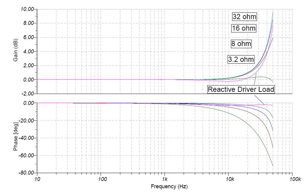
The 60dB high peaking shown in the simulation requires a very high Q output filter.
Obviously the lossy components of real circuitry are missing in the simu: Coil resistance, rdson of power MOSFET, ESR of blocking caps and the likes.....
Peaking in reality is much lower!
Obviously the lossy components of real circuitry are missing in the simu: Coil resistance, rdson of power MOSFET, ESR of blocking caps and the likes.....
Peaking in reality is much lower!
Last edited:
3116 is bd modulation, but can be 1spw. But which of the be confidurations is it?
Is the output filters fully differential? Or are they, as I have read a "pseudo-differential BD modulation"? Or are they SE?
Clarification will be helpful in getting me past page 2!!! 🙂
Am I right in thinking it is " ternary"?
Does it go:
(Internal IC)
Fully differential out of phase -> differential in phase.
(External IC)
Output differential in phase -> differential ended output BTL. ??

Hi all,
here is my issue:
My brother just give me speakers he made
I red a lot of thinks about filters
I don't know anything about it
I want to optimise my YJ 3116 for theses speakers
what can be a good starting point?
here is my issue:
My brother just give me speakers he made
I red a lot of thinks about filters
I don't know anything about it
I want to optimise my YJ 3116 for theses speakers
what can be a good starting point?
This is for Xrk971 and Lo_Tse.
You mentioned having got a board like my 3116 "HSDZ" i.e YJ blue copy... so you may be able to answer my question, as the board does not seem to starground under chip.
The SDZ pin goes through the 100k resistor, then to the PVCC which comes down from the PVCC input (parallel to end of chip under heatsink).
This PVCC joins trace to DC coupling cap GND through 10nf nearest PVCC / 100nf MIDDLE /1nf nearest SDZ resistor).
Now I've removed the 10nf from here to replace between the two power traces underside of board so both PVCC supplies benefit. And I put the 1nf nearest PVCC pin instead, leaving the cap gap nearest SDZ resistor empty.
Anyhow, my question is..... Is this a half-arsed attempt at the "resister/cap to GND" Off of this SDZ to PVCC trace that's in the 3116 Data sheet?
As I now have a "spare" empty "cap gap" between the PVCC trace and GND, I am considering putting the Datasheet SDZ 3.3R/100nf here instead. Will this work in a similar way to the "Giancario" circuit in Wiki?
Last edited:
Nope.
You should use the circuit i posted some posts before. It's a modified version of this circuit which works PVCC independent and use less parts.
You should use the circuit i posted some posts before. It's a modified version of this circuit which works PVCC independent and use less parts.
This is for Xrk971 and Lo_Tse.
You mentioned having got a board like my 3116 "HSDZ" i.e YJ blue copy... so you may be able to answer my question, as the board does not seem to starground under chip.
The SDZ pin goes through the 100k resistor, then to the PVCC which comes down from the PVCC input (parallel to end of chip under heatsink).
This PVCC joins trace to DC coupling cap GND through 10nf nearest PVCC / 100nf MIDDLE /1nf nearest SDZ resistor).
Now I've removed the 10nf from here to replace between the two power traces underside of board so both PVCC supplies benefit. And I put the 1nf nearest PVCC pin instead, leaving the cap gap nearest SDZ resistor empty.
Anyhow, my question is..... Is this a half-arsed attempt at the "resister/cap to GND" Off of this SDZ to PVCC trace that's in the 3116 Data sheet?
As I now have a "spare" empty "cap gap" between the PVCC trace and GND, I am considering putting the Datasheet SDZ 3.3R/100nf here instead. Will this work in a similar way to the "Giancario" circuit in Wiki?
I am afraid that I cannot provide any help. I took a brief listen of the board and found it sounded kind of flat. I put it aside and did not bother to investigate further.
Good luck.
- Home
- Amplifiers
- Class D
- TPA3116D2 Amp