I have wanted a convenient power amplifier that could be used for stereo playback, multi-channel playback, or in a powered speaker. However, this project has been on hold for about a year. For continuity, my original posts on this subject can be found at the following link. Also, thank you to members AndrewT, marce, and tomchr for their previous responses and helpful links.
http://www.diyaudio.com/forums/chip-amps/251542-lm4780-pcb-layout.html#post3866237
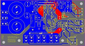
The following layout is meant to provide configuration options (stereo or parallel amplification) when using a stand-alone LM4780. The inputs could include RCA or XLR connections (via an external THAT 1200 board). The potential sources are a preamp, a music player, or an Analog devices ADZS-21469 DSP evaluation board.
The layout below is based on the Texas Instruments (LM3886 and LM4780) data sheets and National Semiconductor application notes (AN-1192 and AN-1849). The output inductor and resistor are connected off-board following the placement considerations raised in chapter 8 (starting on page 235) of Douglas Self's "Audio Power Amplifier Design Handbook 5th edition". The on-board grounding scheme follows the Taming the LM3886 Chip Amplifier article by tomchr on the Neurochrome website and allows for off-board grounding if needed.
While the general layout is basically settled, there are a few questions that I would like to resolve.
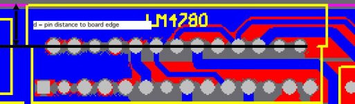
Q1.) What is enough space for heat sink mounting? Can anyone verify the spacing between the back hole centers of the LM4780 and the back edge of the board? For reference, I am using 160 mils as pictured.
Q2.) What is the typical spacing between the power rails to satisfy clearance and creepage safety requirements? For example, figure 40 of the LM4780 data sheet layout appears to use approximately 40 to 45 mil spacing while tables two and three of "Safety Considerations in Power Supply Design" recommend 16 to 47.2 mil (or 0.4 to 1.2 mm) depending on functional needs and pollution level.
Safety Considerations in Power Supply Design
http://www.ieee.li/pdf/essay/safety_considerations_in_power_supply_design.pdf
Q3.) Are there better small signal and ground plane routing alternatives? In the example below, the small signal wires are on the bottom of the board and higher voltage signals are carried on the top. Can anyone provide measurements or experiences when routing the small signals on top and using an isolated small signal ground plane on the bottom?
http://www.diyaudio.com/forums/chip-amps/251542-lm4780-pcb-layout.html#post3866237
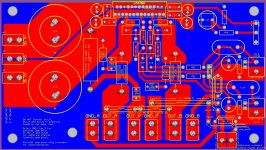
The following layout is meant to provide configuration options (stereo or parallel amplification) when using a stand-alone LM4780. The inputs could include RCA or XLR connections (via an external THAT 1200 board). The potential sources are a preamp, a music player, or an Analog devices ADZS-21469 DSP evaluation board.
The layout below is based on the Texas Instruments (LM3886 and LM4780) data sheets and National Semiconductor application notes (AN-1192 and AN-1849). The output inductor and resistor are connected off-board following the placement considerations raised in chapter 8 (starting on page 235) of Douglas Self's "Audio Power Amplifier Design Handbook 5th edition". The on-board grounding scheme follows the Taming the LM3886 Chip Amplifier article by tomchr on the Neurochrome website and allows for off-board grounding if needed.
While the general layout is basically settled, there are a few questions that I would like to resolve.
Q1.) What is enough space for heat sink mounting? Can anyone verify the spacing between the back hole centers of the LM4780 and the back edge of the board? For reference, I am using 160 mils as pictured.
Q2.) What is the typical spacing between the power rails to satisfy clearance and creepage safety requirements? For example, figure 40 of the LM4780 data sheet layout appears to use approximately 40 to 45 mil spacing while tables two and three of "Safety Considerations in Power Supply Design" recommend 16 to 47.2 mil (or 0.4 to 1.2 mm) depending on functional needs and pollution level.
Safety Considerations in Power Supply Design
http://www.ieee.li/pdf/essay/safety_considerations_in_power_supply_design.pdf
Q3.) Are there better small signal and ground plane routing alternatives? In the example below, the small signal wires are on the bottom of the board and higher voltage signals are carried on the top. Can anyone provide measurements or experiences when routing the small signals on top and using an isolated small signal ground plane on the bottom?
Attachments

Last edited:
Make your Signal ground/Return separate from the Power Ground.
It's not so important with a mono-block, but becomes very important for a multi-channel amplifier.
Do your really need 3 electrolytics for MF supply rail decoupling?
It's not so important with a mono-block, but becomes very important for a multi-channel amplifier.
Do your really need 3 electrolytics for MF supply rail decoupling?
Also, thank you to members AndrewT, marce, and tomchr for their previous responses and helpful links.
You're quite welcome. Thank you for the recognition. Your layout looks eerily familiar to where I landed with the Parallel-86 layout, at least in terms of component placement. There's room for improvement, however.
First off, I suggest revisiting the decoupling network. Andrew hints at that as well. While it may not be strictly necessary, I do support you decision to use decoupling at either end of the chip. I wasn't quite comfortable leaving the far end without decoupling either... However, I don't think you get much benefit from using two small electrolytic cans for the 1-100 kHz decoupling. You can run a simulation to verify, but in my experience, you will get a better decoupling network with a large electrolytic can (1000-2200 uF), a smaller electrolytic can (22 uF) and the largest X7R ceramic cap that you can find. All the caps need to be as close to the IC as possible - so scoot your Zobel resistor out of the way and move the decoupling closer to the IC.
I suggest using a ground plane rather than pours. Move the signal traces to the top of the board and put the ground plane on the bottom. Make the plane as big as you can possibly get, preferably, cover the entire bottom with copper.
The feedback ground and input ground need to stay separate. Connect these to a copper pour (on the top layer if you can fit it in) and connect this pour with a low-inductance trace/pour to the GND at the speaker terminal. If the components that connect to the feedback and input ground poke through the ground plane (they will if the plane covers the entire board), don't forget to remove the connections from these components to the ground plane. Otherwise you'll have a ground loop...
The inputs could include RCA or XLR connections (via an external THAT 1200 board).
Wait a few weeks and I can get you hooked up with one of those THAT boards.
Q1.) What is enough space for heat sink mounting? Can anyone verify the spacing between the back hole centers of the LM4780 and the back edge of the board? For reference, I am using 160 mils as pictured.
I'd leave 0.5 mm (~20-25 mils) minimum between the edge of the board and the heat sink. The distance between the mounting holes can be calculated from the dimensions listed in the LM4780 data sheet. It works out to just over an inch.
Q2.) What is the typical spacing between the power rails to satisfy clearance and creepage safety requirements?
Depends... For a PCB with solder mask, 40 V/mil is normally considered safe. I would never go that tight, though. I also forget if that's the breakdown voltage or the "safe rule of thumb". Google it... 🙂 On a low-voltage board, such as the LM3886/LM4780, 15 mils between planes/pours is plenty.
For PCBs without solder mask, all bets are off... Better use some form of conformal coating for those.
Can anyone provide measurements or experiences when routing the small signals on top and using an isolated small signal ground plane on the bottom?
See my Modulus-86 or Parallel-86.
Tom
Make your Signal ground/Return separate from the Power Ground.
It's not so important with a mono-block, but becomes very important for a multi-channel amplifier.
Hello AndrewT,
Thank you for the feedback. To clarify, the layout is intended to accommodate single board operation (meaning on-board ground point) or multiple board operation (meaning primarily off-board ground point). For this layout, the small signal ground routing is dependent on how RG_A, RG_B and the corresponding jumpers jmp_gndA and jmp_gndB are connected.
For single board operation, the signal ground routes to the load return (black speaker terminal) and the load return is routed to the onboard power ground. This scheme follows the approach presented by tomchr LM3886 chip amp grounding.
For multiple board operation, the signal ground can be connected off-board to the power supply (via the connection terminals in the bottom right hand corner) and the load return is also connected to the off board power supply. This scheme follows the example presented by Douglas Self in figure 18.1 on page 485 of "Audio Power Amplifier Design Handbook 5th edition".
Is this what you were referring to or is there something else?
Do your really need 3 electrolytics for MF supply rail decoupling?
I chose to add additional electrolytics for a variety of reasons.
To support the parallel operation decoupling scheme recommended in figure 16 on page 14 of AN-1192.
To avoid potential problems due to the somewhat narrow V+ trace running along the LM4780 in this layout. Years ago I had a course where we laid out pcbs to support a Motorola Coldfire running at 40MHz on a 2-layer board. There was an example where failure to provide capacitors at each of the power points of the external dynamic RAM caused problems. Granted this is not a fair comparison but it was a motivator.
Based on my interpretation of the presentation marce posted a link to last year. For convenience, the portion regarding multiple capacitors and placement, starts on page 53 of the pdf linked below:
http://www.pcbcarolina.com/images/01_pcb_power_decoupling_myths_debunked.pdf
You can also just model the trace inductance (use one of the many on-line calculators) and run a simulation of the supply impedance in your favorite circuit simulator. That's what I did on my Taming the LM3886 Supply Decoupling page.
I agree with your observations on the skinny V+ trace...
Tom
I agree with your observations on the skinny V+ trace...
Tom
Hello tomchr,
Thank you for the detailed response. I wanted to post yesterday but ran out of time. Starting from the top of the first response.
To me, the appeal of the National board was that some of the measurements provided in the data sheet were based on the layout of the demo board shown (according to Note 11 on page 4 and on page 15). I was also more familiar with the routing strategy employed. Problems I found with this scheme included limited room to optimally mount the chip on a large heat sink (not too tough to overcome) and the routing challenges presented by the addition of pairs of Cc, Rf2, and Cf2.
I was first exposed to your layout when AndrewT recommended your http://www.diyaudio.com/forums/chip-amps/252436-lm3886-pcb-vs-point-point-data.html thread last year. The measurements provided as you flushed out the design (starting at post 30), the layout starting at post 181 http://www.diyaudio.com/forums/chip-amps/252436-lm3886-pcb-vs-point-point-data-19.html, and the comments provided by KSTR and marce were compelling. Two concerns I have for employing this approach with the LM4780 are the narrow trace for V+ and the impact on crosstalk performance for a stereo configuration.
Initially I had a layout similar to the National board that included all of the components I wanted to support two channel or parallel operation. It looked sort of like the LM4780 Pro PCB. However, there were a number compromises I had to make and putting the power connection on the left side made the routing easier. Once I saw Parallel86 was working with this scheme (in particular the relatively narrow V+ trace), I began working out a means to address the stereo layout requirements.
Time permitting, I will try some of your recommendations this weekend or next.
Looking forward to see your THAT 1200 implementation. The board I did is two channel and supports most of the connection options in the data sheet. My layout for the THAT 1200 board is fairly basic and only employed one pour for the ground at the power terminals. Eventually, I intend to compare it (meaning measure and listen) to a pair of Jensen JT-11P-1 transformers.
To clarify my earlier question. The back row of my LM4780 footprint holes are at position zero and my keep out layer is 160mils away to allow room for the heat sink. What distance (dimension d in the attached picture) have you found is good to allow room for the heat sink and maximize the trace width?
Thank you for the detailed response. I wanted to post yesterday but ran out of time. Starting from the top of the first response.
The layout should look familiar. When I surveyed the approaches to component placement and layout of the LM4780, I found the examples typically looked like the National board shown in figure 40 of the data sheet, your component placement approaches (Parallel-86: High-power composite amplifier achieving 0.00020 % THD. and Modulus-86 Rev. 2.0: Composite amplifier achieving 0.00014 % THD.), the Chipamp Electronics layout, and combinations of the first two approaches (e.g. the LM4780 Pro PCB on moutoulos ? - LM4780 Pro PCB… Your layout looks eerily familiar to where I landed with the Parallel-86 layout, at least in terms of component placement.
To me, the appeal of the National board was that some of the measurements provided in the data sheet were based on the layout of the demo board shown (according to Note 11 on page 4 and on page 15). I was also more familiar with the routing strategy employed. Problems I found with this scheme included limited room to optimally mount the chip on a large heat sink (not too tough to overcome) and the routing challenges presented by the addition of pairs of Cc, Rf2, and Cf2.
I was first exposed to your layout when AndrewT recommended your http://www.diyaudio.com/forums/chip-amps/252436-lm3886-pcb-vs-point-point-data.html thread last year. The measurements provided as you flushed out the design (starting at post 30), the layout starting at post 181 http://www.diyaudio.com/forums/chip-amps/252436-lm3886-pcb-vs-point-point-data-19.html, and the comments provided by KSTR and marce were compelling. Two concerns I have for employing this approach with the LM4780 are the narrow trace for V+ and the impact on crosstalk performance for a stereo configuration.
Initially I had a layout similar to the National board that included all of the components I wanted to support two channel or parallel operation. It looked sort of like the LM4780 Pro PCB. However, there were a number compromises I had to make and putting the power connection on the left side made the routing easier. Once I saw Parallel86 was working with this scheme (in particular the relatively narrow V+ trace), I began working out a means to address the stereo layout requirements.
There's room for improvement, however.
Time permitting, I will try some of your recommendations this weekend or next.
Wait a few weeks and I can get you hooked up with one of those THAT boards.
Looking forward to see your THAT 1200 implementation. The board I did is two channel and supports most of the connection options in the data sheet. My layout for the THAT 1200 board is fairly basic and only employed one pour for the ground at the power terminals. Eventually, I intend to compare it (meaning measure and listen) to a pair of Jensen JT-11P-1 transformers.
I'd leave 0.5 mm (~20-25 mils) minimum between the edge of the board and the heat sink. The distance between the mounting holes can be calculated from the dimensions listed in the LM4780 data sheet. It works out to just over an inch.
To clarify my earlier question. The back row of my LM4780 footprint holes are at position zero and my keep out layer is 160mils away to allow room for the heat sink. What distance (dimension d in the attached picture) have you found is good to allow room for the heat sink and maximize the trace width?
Attachments
You could straighten all the +V and -V leads to bring them out above the PCB. Then wire these up separately using a mini power PCB with the decoupling added to this mini board.
To clarify my earlier question. The back row of my LM4780 footprint holes are at position zero and my keep out layer is 160mils away to allow room for the heat sink. What distance (dimension d in the attached picture) have you found is good to allow room for the heat sink and maximize the trace width?
According to the package drawing in the data sheet, the distance from the center of the rear row of pins to the back of the package is 166 mil (+/- 10 mil). I'm pretty sure I placed the rear row of pins 125 mil from the board edge.
~Tom


I'd probably swap the Thiele network and the Zobel capacitor on the left side to reduce the trace length in the Zobel a bit. It's a bit academic, but you might as well optimize it.
I'd probably play a bit more with the placement of the feedback and input components. I suspect you can clean that up and get the output pours to flow a bit better (maybe under the input resistors).
BTW, to make the parallel play nicely, you need as low a DC gain as you can get away with. Either by using a cap in the feedback circuit or by using a DC servo.
Tom
Hello Tom,
Thank you for your suggestions and for pointing out potential problems when using a parallel output. I wanted to avoid the additional parts for a DC servo but I am less interested in putting another cap in the feedback path. I think you posted it somewhere but what opamp and network would you recommend for the DC servo?
Also, why did you select what appears to be parallel 1000uF 6.3V caps for each return leg on your parallel86?
The challenge with a parallel amp is to get the channels to play nicely together. By "nicely" I mean that in the ideal world, there should be no current flowing between the two amp channels. In practice, that's not possible. This is why you use ballasting resistors (0.1 Ω) on the outputs of the amps. This allows the difference in output offset voltage to be distributed across the ballasting resistors. This also sets up an offset current in the ballasting resistors. If this current becomes too large, the amp performance will suffer as the output swings near the supply rail. This is because some of the output current of the amp will supply the load and some of the output current will supply the other half of the parallel pair. If not designed properly, it is possible to have over 1 A flowing in the ballasting resistors! Been there, done that, took the measurements, got the T-shirt, didn't like it.
To minimize the offset current, the output voltage offset must be minimized. For a straight parallel amp, this is pretty easy to do with a DC servo. Just add a DC servo to each half of the amp and call it good. If you don't like the complexity that comes with a DC servo, you can use a capacitor to reduce the amp gain to 1 V/V at DC. This limits the output voltage offset to 1*Vos, which for the LM3886/LM4780 is 10 mV worst case and 1 mV typical (AFAIR). With two 0.1 Ω ballasting resistors, the worst case offset current is now 100 mA. Typical case 10 mA.
In a composite parallel amp, such as the Parallel-86, life gets even more complicated. The Parallel-86 uses a global DC servo to ensure that the output offset of the entire composite amp is as close to 0 V as possible. This requires the "inner amp" to have some non-zero gain at DC. This rules out a DC servo on the "inner amp".
Now, to the first part of your question: "How do you design a high-performance DC servo?" DC servo design is an often neglected part of the amplifier design. Most designers slap on a standard circuit and call it good. However, a good DC servo is designed to provide as little THD contribution as possible within the audio band. I spent quite a while optimizing the DC servo for the Modulus-86 Rev. 2.0 and Parallel-86 to ensure that I had stellar THD at 20 Hz for the overall amp.
The DC servo design is a compromise between THD contribution within the audio band and settling time. The DC servo in my Modulus-86 Rev. 1.0 settles in a couple of minutes. It's a simple integrator servo. The DC servo in the Modulus-86 Rev. 2.0 settles in about 10 seconds and adds no THD above 20 Hz. It's employs 3rd order filtering to accomplish this.
The op-amp(s) in the DC servo will need to have low input offset voltage and low input bias current. In other words, they need to provide good performance when used as an integrator. The best candidate I've found is the OPA277.
I can't recommend a generic plug-n-play circuit. If you want good performance, you'll have to design something... For a LM3886/LM4780 amp, you can probably start from the generic integrator DC servo and see if that provides good enough performance. That's not something I've looked at in detail as I went straight to the composite amps for better performance.
Tom
Gootee did a very big and good contribution to a Thread on DC servos.
I think he also has a website.
He included an LT spice simulation in there.
I think he also has a website.
He included an LT spice simulation in there.
That he did. That was my starting point as well. Here's the thread: http://www.diyaudio.com/forums/chip-amps/107246-dc-servo-question.html
Bonnie Baker's app note on stop band limitations of Salen-Key filters is a worthwhile read as well: http://www.ti.com/lit/an/slyt306/slyt306.pdf
There are a couple of pages on the DC servo in Bob Cordell's book as well.
I don't think you have to be as fancy as Mr. Gootee or me. My gut feel is that you'll probably get the performance you need (i.e. as good as the naked LM4780) using a regular integrator if you set the overall amplifier cutoff somewhere in the 0.1-1 Hz range. You can run a sim or build and measure to make sure.
Tom
Last edited:
… If this current becomes too large, the amp performance will suffer as the output swings near the supply rail. This is because some of the output current of the amp will supply the load and some of the output current will supply the other half of the parallel pair. If not designed properly, it is possible to have over 1 A flowing in the ballasting resistors! Been there, done that, took the measurements, got the T-shirt, didn't like it.
Hello Tom,
Thank you for providing a detailed response including your experiences using the ballast resistors only. This goes beyond what is provided on page 11 of AN-1192. It was also helpful to review AN-1192 since I realized that a parallel configuration will likely require an input buffer to compensate for the reduced input impedance.
Now, to the first part of your question: "How do you design a high-performance DC servo?" DC servo design is an often neglected part of the amplifier design. Most designers slap on a standard circuit and call it good. However, a good DC servo is designed to provide as little THD contribution as possible within the audio band. I spent quite a while optimizing the DC servo for the Modulus-86 Rev. 2.0 and Parallel-86 to ensure that I had stellar THD at 20 Hz for the overall amp.
The DC servo design is a compromise between THD contribution within the audio band and settling time. The DC servo in my Modulus-86 Rev. 1.0 settles in a couple of minutes. It's a simple integrator servo. The DC servo in the Modulus-86 Rev. 2.0 settles in about 10 seconds and adds no THD above 20 Hz. It's employs 3rd order filtering to accomplish this.
The op-amp(s) in the DC servo will need to have low input offset voltage and low input bias current. In other words, they need to provide good performance when used as an integrator. The best candidate I've found is the OPA277.
I can't recommend a generic plug-n-play circuit. If you want good performance, you'll have to design something... For a LM3886/LM4780 amp, you can probably start from the generic integrator DC servo and see if that provides good enough performance. That's not something I've looked at in detail as I went straight to the composite amps for better performance.
Tom
The Electronics Now article (https://ia601701.us.archive.org/15/...s_1992-11/Radio_Electronics_November_1992.pdf) on composite amplifiers looks interesting and I will give it a read. Also, the article on pages 47-56 was very similar to an old lab assignment. For now, I am not interested in attempting your Modulus-86 Rev. 2.0: Composite amplifier achieving 0.00014 % THD. or Parallel-86: High-power composite amplifier achieving 0.00020 % THD. approach but I may attempt it later in the year if the standard amp is unsatisfactory. Out of curiosity, did you determine your filter values working backward from the combined Bode plot created in simulation?
Gootee did a very big and good contribution to a Thread on DC servos.
I think he also has a website.
He included an LT spice simulation in there.
That he did. That was my starting point as well. Here's the thread: http://www.diyaudio.com/forums/chip-amps/107246-dc-servo-question.html
Hello Andrew and Tom,
Thank you both for suggesting and providing a link to Gootee's posts on DC servos. I will take a look after a review of Sedra and Smith's coverage of integrators and differentiators. Chapter 16 of Douglas Self's Audio Power Amplifier Design Handbook (5th edition) also covers DC servo design. The 2C integrator in his book (figure 16.4) uses the same basic topology as presented in AN-1192. However, the resistor values are an order of magnitude different for the same size capacitors. I need to work out why. Also, figures 16.2 and 16.6 can be combined to provide additional nulling.
At this point, I will probably stick with the standard servo example in figure 13 on page 12 of AN-1192 and figures 16.2, 16.4 (and maybe 16.6) of Douglas Self's book . Since this will require regulators, I will add an oboard THAT 1200 series for each channel. However, I am not sure if a buffer (U7 in figure 13 of AN-1192) is required or if I can use the THAT1200 to drive the parallel load directly. I need to verify this.
An additional concern is related to the ground connection for the DC servo and the THAT 1200. Since the DC servo circuit and the THAT 1200 are in the feedback and signal path, it seems both should be grounded directly to the signal common ground and routed to speaker return (black lead). Is this what you would recommend?
Regards,
Jeremy
Last edited:
Thank you for providing a detailed response including your experiences using the ballast resistors only.
You're welcome.
It was also helpful to review AN-1192 since I realized that a parallel configuration will likely require an input buffer to compensate for the reduced input impedance.
I'm not sure that's true. In a parallel amp where both amp halves are non-inverting, I don't think you need an input buffer. I glanced quickly through the LM3886 data sheet, but didn't find an input impedance spec. The input is an emitter follower into a diff pair, so it should be fairly high impedance (a few MΩ at least). As long as your source can supply the input bias current, I think you'll be fine.
Now if you're using the inverting configuration for the two amp halves, you're right. You will need an input buffer as you're likely looking at something like a 500-1000 Ω input impedance.
Out of curiosity, did you determine your filter values working backward from the combined Bode plot created in simulation?
The battle box looks as follows:
1) The settling time of the DC servo is inversely proportional to the cutoff frequency of the servo. You want a low settling time (-> high cutoff frequency) to ensure that the amp recovers fast from the turn-on transient.
2) You want the DC servo to contribute as little THD as possible at 20 Hz.
Requirement 1) sets the lower limit on the cutoff frequency. I'd prefer the amp to be fully settled within a few (say <10) seconds of power-up. Depending on the DC gain of your amp, you'll find that you need a cutoff frequency above 0.1-1 Hz Hz to satisfy this requirement. Note that the DC servo cutoff frequency will "see" the Miller effect due to the LM3886/LM4780 amp gain. This gives you a fair amount of wiggle room on the cutoff frequency (and introduces ambiguity on what exactly the cutoff frequency is).
Requirement 2) sets the higher limit on the cutoff frequency. I determined this point by simulation and verified it in the lab. Basically, dial up the cutoff frequency of your servo until you start seeing a rise in THD at 20 Hz. Chose a cutoff frequency slightly below this value. This is trivial to do in simulation.
On MOD86 R1.0, I followed requirement #2 only. I was aiming for the best THD I could get and decided to let the settling time fall where it may. For MOD86 R2.0, I took the next step and implemented 3rd order filtering in the DC servo to meet both requirements.
A well-designed LM3886/LM4780 layout will deliver THD that's quite a bit higher than my MOD86, so Requirement #2 for the DC servo in case of a naked LM3886/LM4780 amp is not as stringent. That's probably why you can get away with a regular integrator (1st order filtering). Either that or nobody has bothered optimizing the DC servo... That is possible... 🙂
Also, figures 16.2 and 16.6 can be combined to provide additional nulling.
I don't have those figures committed to memory. Just be careful not to get too caught up in the DC servo game. The best you can do is Vos_out = Vos*Av, where Vos_out is the offset voltage on the output of your total amplifier, Vos is the input referred offset voltage of the integrator op-amp, and Av is the DC gain of the LM3886/LM4780 portion of the amp. This is why you need an op-amp with low DC offset voltage to start with.
An additional concern is related to the ground connection for the DC servo and the THAT 1200. Since the DC servo circuit and the THAT 1200 are in the feedback and signal path, it seems both should be grounded directly to the signal common ground and routed to speaker return (black lead). Is this what you would recommend?
Yep.
Tom
Last edited:
Hello Tom,
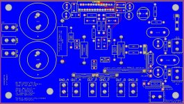
Thank you for the help. The servo version is on hold until the end of the summer. For now, a cleaned up version of the standard stereo version is attached for anyone interested. The parallel option was retained for experimentation (and convenience).
Thank you for the help. The servo version is on hold until the end of the summer. For now, a cleaned up version of the standard stereo version is attached for anyone interested. The parallel option was retained for experimentation (and convenience).
Attachments

- Home
- Amplifiers
- Chip Amps
- LM4780 Stereo or Parallel Evaluation board