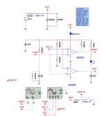
At power-up MUTE is high and SDZ comes up after the inital 10ms power-on-delay within the TPA. After the desired delay MUTE goes low, so amp is working.
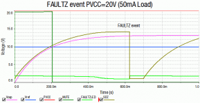
FAULTZ condition latches the outputs to High-Z, SDZ is pulled low to clear the event.
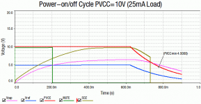
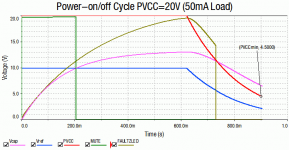
At power-off, SDZ is pulled low before the minimum PVCC is reached.
SDZ can also be pulled low by an external input.
Minumum board.current should be +40mA.
FAULTZ condition latches the outputs to High-Z, SDZ is pulled low to clear the event.
At power-off, SDZ is pulled low before the minimum PVCC is reached.
SDZ can also be pulled low by an external input.
Minumum board.current should be +40mA.
Well, better go this way. 🙂
Almost same behaviour as "final answer" with the benefits of an led-indicator.
Almost same behaviour as "final answer" with the benefits of an led-indicator.
Attachments
Last edited:
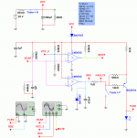
Revisited the supervisor idea.

This one gives you an absolute PVCC undervoltage lockout, and 200mS /SD to unmute delay, and less parts than anything else.
This one gives you an absolute PVCC undervoltage lockout, and 200mS /SD to unmute delay, and less parts than anything else.
SDZ-mute on power-on does not work properly to knowledge.
Edit: The Problem at PFI is, that the trip-poin scales with PVCC, so this input works only for one voltage atm. As the z-diode keeps VDD at ~the same level, undervoltage at this pin gets only detected when PVCC is at ~4.5V which is the minimum PVCC, SDZ needs to be pulled low before.
To my understanding, it wont work this way.
The "only" thing you have then, is 200ms startup delay and FAULTZ clearing (which also works with SDZ/FAULTZ tied together).
Last edited:
The TPS3707 is fully functional at Vdd=2.0V. So assuming the time constant of the decoupling cap and the PVCC-to-VDD resistor is short compared to the rise time of PVCC, so that VDD reaches 2.0V before PVCC reaches 4.5V, you'll be alright.
And provided PVCC plateaus before the 200mS unmute time expires, you should be OK there too. If it doesn't, PVCC is probably rising slowly enough that the TPA's own PSRR should prevent any bad sounds.
And provided PVCC plateaus before the 200mS unmute time expires, you should be OK there too. If it doesn't, PVCC is probably rising slowly enough that the TPA's own PSRR should prevent any bad sounds.
It does not (prevent), due to the time constants while charging the inputs. You need to look into the DS again.
TIs parameters are for a source-impedance of 0 ohms Even S.E. is problematic.
That TVS thing is supposed to not gonna work.
TIs parameters are for a source-impedance of 0 ohms Even S.E. is problematic.
That TVS thing is supposed to not gonna work.
Last edited:
Gmarsh what are the apps and requirements for this amplifier anyhow? eg typical sources and speakers?
my guess or most information I can gather, since you decided to use TDA3118 and other top sided cooling isn't designed in place
inputs > stereo SE floating > ipod or mp3 player
outputs 20Wx2 (6-8ohms) > 4" full range not 4 ohm car stereo speakers
power 16-24 V independent power source > (2 wire laptop bricks or 2x12V battery no charger)
Last edited:
package = Hammond 1455L1202
.079 slot for 0.062" PCB X 100 mm X xxx mm
using lowest slot allows 20 mm max component height
input 2X RCA panel mount connectors ?
output 4 x ?
power 1 x ?
volume pot ?
led indicator tricolor panel mount
power switch ?
fuse ?
.079 slot for 0.062" PCB X 100 mm X xxx mm
using lowest slot allows 20 mm max component height
input 2X RCA panel mount connectors ?
output 4 x ?
power 1 x ?
volume pot ?
led indicator tricolor panel mount
power switch ?
fuse ?
Fuse + TVS-Diode? 🙂
Btw. Going for an ATtiny4.
probably a good idea, if using 2x batteries in series with chargers / PV panels connected = poof
This card will be able to drive music into 4 ohms easily.Gmarsh what are the apps and requirements for this amplifier anyhow? eg typical sources and speakers?
my guess or most information I can gather, since you decided to use TDA3118 and other top sided cooling isn't designed in place
inputs > stereo SE floating > ipod or mp3 player
outputs 20Wx2 (6-8ohms) > 4" full range not 4 ohm car stereo speakers
power 16-24 V independent power source > (2 wire laptop bricks or 2x12V battery no charger)
TPA3116/TPA3118 ICs share the same die, provided the die is cooled sufficiently to keep it below Tj(max) then you're OK. TPA3116 has a Phi-jb of 5.7 deg C/watt, TPA3118 is 4.8 deg C/watt... this is the thermal resistance of the part to the thermal pad on the device, so there's no package limitation.
Pretty much every chinese amp out there uses a "DIP14/16" sized stick-on heatsink, which has a thermal resistance of around 50 degrees C/watt in natural convection. Example heatsink:
V5619A Assmann WSW Components | AE10812-ND | DigiKey
I rarely hear reports of these cards overheating when people are using them for ordinary music listening. Based on all of that, the TPA seems to be getting by just fine as an audio amplifier with an effective Rja of 55 degrees C/watt.
My PCB design is at the very least comparable to the "old board" mentioned in section 4.2 of this document, which has a ~45 degrees/watt Rja, or say, a 40 degC/watt case to ambient assuming a 5 degC/watt junction to ambient.
http://www.ti.com/lit/an/snva183b/snva183b.pdf
The "old board" only has 2sq inches of bottom side copper, I've got 7. So I'm already better than most of the chinese TPA3116 boards out there at getting heat out of the chip.
Now if you really want to do good, buy one of these guys and stick it to the PCB underneath the TPA3118, then bolt the card to a metal chassis:
H48-6-45-25-4-1A t-Global Technology | 1168-1701-ND | DigiKey
This is what I did on the red Boominator card where I was experimenting with a 12->24V DC/DC and "class D/G" operation. I had the TPA3118 outputting 50Wrms sine into power resistors, out of both channels, with the DC/DC converter also dumping heat into the PCB, using just the Hammond 1590N case as the heatsink. It ran overnight with no problems.
The card won't fit the card guides of a 1455L case, bolt it to the removable bottom with 1/8" standoffs. Interior height is 27.5mm, subtract 3.2mm for the standoffs and 1.6mm for the PCB thickness and you're at 22.7mm from top of PCB to bottom of the roof. So a 20mm cap is fine, and has 2.7mm of vent space above it.package = Hammond 1455L1202
.079 slot for 0.062" PCB X 100 mm X xxx mm
using lowest slot allows 20 mm max component height
input 2X RCA panel mount connectors ?
output 4 x ?
power 1 x ?
volume pot ?
led indicator tricolor panel mount
power switch ?
fuse ?
Power switch? fuse? connectors? use whatever you want. This card is intended to drop in place of an EVM or a YJ card, not to be a full-featured finished product.
I had an AVR on here initially, and I'd throw one on in a heartbeat, but bare PCB buyers would need AVR programming tools.Fuse + TVS-Diode? 🙂
Btw. Going for an ATtiny4.
I s'pose I could preprogram parts and include them with the PCB..
Ya, we'd thought about an ATTiny4/10 in SOT23-6 so we can have MUTE-Delay/SDZ and Power-off fastmute.
In the end, price compared to a 393 solution would be the same. I'd do my circuit idea with resistor-arrays, thats why they're all 220k or a multible.
In the end, price compared to a 393 solution would be the same. I'd do my circuit idea with resistor-arrays, thats why they're all 220k or a multible.
TPA3116 has a Phi-jb of 5.7 deg C/watt, TPA3118 is 4.8 deg C/watt... this is the thermal resistance of the part to the thermal pad on the device
thanks ,this is the key that escaped me. In conclusion , the TPA3118 is superior in every way if done "properly". edit> err , what is the estimated Theta J for package tru vias to the bottom PCB ground plane, and is the solder bonded to the package in our build?
I was thinking of using this amp PCB and DAC using some +/-12 V common supply
for working to some PC stuff, so id need a true differential interface located off on a cleaner ground.
Last edited:
This card will be able to drive music into 4 ohms easily.
TPA3116/TPA3118 ICs share the same die, provided the die is cooled sufficiently to keep it below Tj(max) then you're OK. TPA3116 has a Phi-jb of 5.7 deg C/watt, TPA3118 is 4.8 deg C/watt... this is the thermal resistance of the part to the thermal pad on the device, so there's no package limitation.
Pretty much every chinese amp out there uses a "DIP14/16" sized stick-on heatsink, which has a thermal resistance of around 50 degrees C/watt in natural convection. Example heatsink:
I rarely hear reports of these cards overheating when people are using them for ordinary music listening. Based on all of that, the TPA seems to be getting by just fine as an audio amplifier with an effective Rja of 55 degrees C/watt.
My PCB design is at the very least comparable to the "old board" mentioned in section 4.2 of this document, which has a ~45 degrees/watt Rja, or say, a 40 degC/watt case to ambient assuming a 5 degC/watt junction to ambient.
http://www.ti.com/lit/an/snva183b/snva183b.pdf
The "old board" only has 2sq inches of bottom side copper, I've got 7. So I'm already better than most of the chinese TPA3116 boards out there at getting heat out of the chip.
We ran some tests with our small TPA3132D2 board, which gives solid 50W (2x25W) continous output power at 8R wih PVCC=23.5V. Measured with 30Hz sine. This was measured near the thermal shutdown tripping point. 🙂
To quote myself from here:
http://www.diyaudio.com/forums/class-d/251859-building-tpa3132-amp-board-6.html#post4213925
So lets see:
Ideal:
TPA3132 = 8R/(8R+0R12+0R12) = 0.97 = 97%
TA = 18°C
Pout = 50W
Efficiency: 👎 = 97%
Rth_JA = 31K/W
Pdiss = (50W / 0.97) - 50W = 1.54W
TC = TA + Pdiss * Rth_JA = 18°C + 1.54W * 31K/W = 66°C
Well, we wont have that 97% in practice, so lets assume 92%:
Pdiss = (50W / 0.92) - 50W = 4.34W
TC = TA + Pdiss * Rth_JA = 18°C + 4.34W * 31K/W = 152.54°C
For 140°C:
Pout(TC)=[n*(TC-TA)] / [Rth_JA - Rth_JA*n]
Pout(140°C) = [0.92*(140°C-18°C)] / [31K/W - 31K/W*0.92] = 45.25W
So having the correct values from the test:
VCC:23.5V
Iin:2.2A
n=0.92%
Pout: 23V5*2.2A*0.92 = 47.56W
😛
So there wont be any trouble with the TPA3116/3118 on such a big pcb.
Well, we wont have that 97% in practice, so lets assume 92%:
I figure about 3% is due to filter losses eg inductors the other 4-5% is switching losses at the device.
Well, as you might know, my implementation is filterless.
So there's no filter loss but additional loss due to hard switching and increased HF.
So there's no filter loss but additional loss due to hard switching and increased HF.
Last edited:
ugh filterless why increase more RF spray don't you care for the environment?
We already PV micro inverters sprouting up here in my neighborhood like mushrooms.
anyway how would I know what yer doing Im in this thread not yours.
BTW doesn't the speaker network act as a filter, so that must figure in the calcs
We already PV micro inverters sprouting up here in my neighborhood like mushrooms.
anyway how would I know what yer doing Im in this thread not yours.
BTW doesn't the speaker network act as a filter, so that must figure in the calcs
Well, i did measured the radiated HF and compared to the MAX9709. The TPA needs a FB-filter at least, while the MAX9709 does not. The speaker just filters LF, not HF.
- Status
- Not open for further replies.
- Home
- Amplifiers
- Class D
- "Proper" TDA3116 PCB