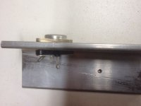
How do you get the heat to the heatsink if you bolt to non-metallic insulators? I know there are cases without the heat generated here, but I would be interested to see how these sockets would be used in this amp.
It goes below the heat sink. Mica insulator with compound goes directly between the case of the device and the sink.
Attachments
It goes below the heat sink. Mica insulator with compound goes directly between the case of the device and the sink.
If a PCB is used, I guess it will go under the heatsink flange and
the socket underneath it?
Dennis
Dear friends of everywhere, recently, later that is my regular characteristic I did think about that people do faster than me. I recheck the CSX1 and the CSX2 but comparing with the original diagram that Mr Pass show in the BAF2013, I noted that there are not capacitors on the signal pathway, maybe for avoid DC current in the secondary of the transformer. Later I said to me that in the source-gate polarization of the Vfet there are not current. Is that true?
The other question is, that capacitor is possible to avoid its use or Do we need a different transformer for use without it?
The other question is, that capacitor is possible to avoid its use or Do we need a different transformer for use without it?
dady , as you well pointed in PM , those 220uF (ref. page 3 sch in art_sony_vfet_pt1.pdf) are in signal path ...... at least sort of ;
however - they're not in signal path in usual manner - right ditto in between two amplification stages , but more in role of voltage shifter/path to virtual gnd
besides that , I'm not overly bothered having Elna Silmic 10uF ditto in signal path , in my Papa's Koan M2 , ZMcleverly bypassed with 1uF polycarbonate (Philips MKC)
so , again , sorry - another Brainfart by Mighty ZM
Last edited:
If a PCB is used, I guess it will go under the heatsink flange and
the socket underneath it?
Dennis
Dennis,
No sockets if PCB is used. PCB is attached to the flange by the screws used to mount the VFETs to the flange.
Regards,
Dan 🙂
yup
however - if you use pcb , avoid sockets
Yep, I have the PCBs and figured they would not work with those, but did want to understand the heat issue.
Thanks for all replies.
After getting my biases in place and minimizing the DC offset on the output. How do I go about or do I need to adjust the RCA offset?
Regards,
Dan 🙂
Regards,
Dan 🙂
RCA offset? You mean the 20 Ohm potmeter of the buffer? I would set that first, so there is no DC through the Jensen.
.......How do I go about or do I need to adjust the RCA offset?
Regards,
Dan 🙂
Attachments
RCA offset? You mean the 20 Ohm potmeter of the buffer? I would set that first, so there is no DC through the Jensen.
Yes. It's a new experience for me dealing with DC offset on an input. I've only ever measured it on the output. I'll fire it up without the SITs and take some measurements.
Regards,
Dan 🙂
Hi guys,
What size L-shaped brackets are you using? I'm thinking of
using 2" x 2" x 0.25" in 11" length but am unsure if that might
be too thick.
Thanks,
Dennis
What size L-shaped brackets are you using? I'm thinking of
using 2" x 2" x 0.25" in 11" length but am unsure if that might
be too thick.
Thanks,
Dennis
Hi guys,
What size L-shaped brackets are you using? I'm thinking of
using 2" x 2" x 0.25" in 11" length but am unsure if that might
be too thick.
Thanks,
Dennis
Dennis,
That exact size has worked well for me.
Regards,
Dan 🙂
Dennis,
That exact size has worked well for me.
Regards,
Dan 🙂
Thanks Dan.
Cheers,
Dennis
Trouble getting my VFETS biased. All supply voltages normal. When adjusting the bias with out SITs the lowest I can get is 6.4VDC. This is probably the cause of myself not being able to get more than .075vdc across R11/R12. I think the cause is the output of my bias supply is too high at 19.8vdc. This is too much for the TL431 circuit?
Regards,
Dan 😕😕
Regards,
Dan 😕😕
- Status
- Not open for further replies.
- Home
- Amplifiers
- Pass Labs
- Article - Sony VFETs part 1