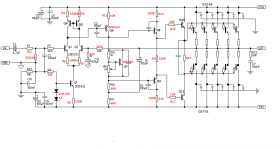
Current mirror on this circuit must be PNP type.
Using bootstrap resistor with triple emitter follower seem useless. VAS output impedance still lower. You can use constant current source for VAS load.
You can consider to use other compensation to increase slew rate and decrease THD at 20kHz.
I do not understand of using 10 ohm resistor series with decoupling cap at output transistor.
You should increase the VAS bootstrap resistors (R10 and R11) to 6k8. With the values you have currently, the VAS will pass a lot of current with 70V rails, and will probably fail without a lot of heatsinking.
~5-10mA standing current through the VAS is ample for an EF3.
Last edited:
Using a pro- amp trafo/PS to power that thing ? (Nice big amp- BTW).
Mine is quite humble , A E- waste logitech trafo with my first toner transfer
PS (4 X 4700u). (below)
The big board is a "protector" - temp./overcurrent/DC/ ...AC even. 🙂
Need to buy the lamps and mount it all on a nice Tennessee OAK board. 😀
(bottom of a moonshine barrel) ...
OS
Tennessee oak is probably pretty flammable.
I can only agree with your approaches to safety, Nigel and Os. I lucked upon an unusual, metered
800VA Grundig KT56 isolated variac some years ago and that makes it safer when I hit the switch too.
It's limited for running up to full power but the retro look on the bench was hard to resist 😎

800VA Grundig KT56 isolated variac some years ago and that makes it safer when I hit the switch too.
It's limited for running up to full power but the retro look on the bench was hard to resist 😎
No neew to worry about safetyu in my case , I have all the necessary measires to keep everything safe starting from fuse blowers various switches etc, and after all even if something goes up in smokes it isnt the first time , secondly I loose only money , thirdly since I know how to work safe for all I care the amp can burn like HELL as long as im not touching it with my fingers 😀😀
But hey burning down amps or tables is not exactly what I have in plan.
bimo you said current mirror should be PNP so you mean from transistors q2 to q3 q4 and q5?
by no need for a bootstrap resistor you mean the two 220R ones at the + supply rail that connect to the current mirror?
But hey burning down amps or tables is not exactly what I have in plan.
bimo you said current mirror should be PNP so you mean from transistors q2 to q3 q4 and q5?
by no need for a bootstrap resistor you mean the two 220R ones at the + supply rail that connect to the current mirror?
Attachments
oh and for the much talked about safety circuits, i have some in plan but hey first you need and amplifier thats working , otherwise there is nothing to protect 😀
and by the way , why noone of you guys commented on the possible topologies i mentioned in my previous posts rather than safety ? 😀
i have seen some older amplifiers have a capacitor coupled output , well definately it has some feedback on the sound quality and bandwith but it's also a safety feature no relay can give to the speaker , since most semiconductors fail to a short circuit mode and since capacitors block DC it is basically the simplest and to my current understanding best speaker protection possible.
about my other ideas please refer to the last paragraph of post #33
if you have the time and will to go into what i said there ofcourse.
also apart from the oldschool approach with solid state output decoupling via capacitor, what can you say about an output transistor stage that is capacitor coupled or in other words has a decoupling capacitor going to each next transistor base? I want to hear some opinions and then i could tell what i think showing my idea in the schematic. basically the idea would be to use direct coupling for the first pairs of the output transistors and then use capacitor coupling for the next pairs, this could reduce the power consumption and unnecessary heating in the output stage also be a little fail safe so that if the output stage base gets full curent instead of all the devices being open just the first pair will be.
what are the drawbacks of such a design?
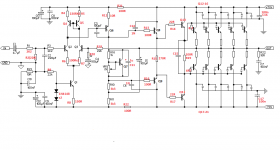
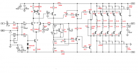
I would say that neither of the p.s. ideas from post 33 are practical or would be beneficial. Comments on the schematic for post 44. 2n5401 pnp's for Q4,5. R13,16 should be in the base circuit of Q8,9 ahead of the capacitors. Change their value to 100 ohms. Using them as they are can cause issues with frequency compensation and will cause loss in available voltage swing, the current limiting they provide is less beneficial than the issues they cause. Change the values of C6 and its twin on the upper half which is not numbered to 1nF. Use MJE340/350 pair for Q8,9. Make R15 270 ohms to keep their idle power reasonable. Add 100 ohm resistors to the rails between the VAS and the first set of drivers to decouple the front end from the output stage. Q10,11 can be MJE15030,15031 pair, with R19 being 100 ohms.
The use of capacitive coupling for anything in this type of topology would only serve to degrade performance.
The use of capacitive coupling for anything in this type of topology would only serve to degrade performance.
Hi Crazy
I had a little time this morning and whipped up this schematic for you.
It should work on a basic level and the rail fuses should at least prevent a fire in the event of a major failure, but won't stop the output transistors going up in smoke 😀
I had a little time this morning and whipped up this schematic for you.
It should work on a basic level and the rail fuses should at least prevent a fire in the event of a major failure, but won't stop the output transistors going up in smoke 😀
Attachments
Coupling capacitor
An AC coupled output would give you very good speaker protection, arguably at the expense of sound quality (I have no experience personally).
The coupling capacitor should be placed between the output transistor emitter resistors and the speaker terminal.
But if you want to do that then you would normally redesign the circuit as single rail (140V) instead of split rail (+/- 70V), and then bias the input so that there is always a polarising voltage (~1/2 Vrail) against the coupling capacitor. This improves sound quality, so I'm told.
Since DC offset stability becomes a non-issue, I would personally simplify the front-end substituting the LTP + current mirror with a single transistor input.
All in all the inclusion of the output coupling capacitor would result in a complete redesign.
Post44.
At last and far too infrequently a properly drawn schematic. Well done.
Note the two different ground symbols.
Note the HF decoupling fitted to the collectors of every output device.
Note the base stoppers on the drivers and output devices.
Compare to post46
At last and far too infrequently a properly drawn schematic. Well done.
Note the two different ground symbols.
Note the HF decoupling fitted to the collectors of every output device.
Note the base stoppers on the drivers and output devices.
Compare to post46
Post 44
Q2, 3 & 6 use inappropriate devices.
Post46
Q1, 2, 4, 5 & 6 use inappropriate devices.
Both posters should look carefully at choosing more suitable input filters for an audio amplifier.
Q2, 3 & 6 use inappropriate devices.
Post46
Q1, 2, 4, 5 & 6 use inappropriate devices.
Both posters should look carefully at choosing more suitable input filters for an audio amplifier.
Last edited:
Post 44
Q2, 3 & 6 use inappropriate devices.
Curious why you feel the 2n5551/5401 and mje340/350 are inappropriate?
Post46
Q1, 2, 4, 5 & 6 use inappropriate devices.
Perhaps you mean post 47.
Last edited:
yes, 44 & 47.
The gain of the 2n is a bit low for input. requires too much bias current. This results in a high voltage at both bases relative to signal ground.
For the mirror you must use a Q that is good at very low Vce, i.e. during near saturated conditions. Some of the BC meet this very special requirement.
The 350 is a high voltage device. Many other devices do not compromise their other parameters as much as the 350 due to having a lower Vce0. We need ultra low Cob and high fT . The 340/350 are rarely specified for these and the many clones give no guarantees to meeting the real devices parameters.
Try Sanyo's TV Q eg 2sa1360 etc.
thanks for the comments on the devices , I must say in this stage im not so concerned about the devices since i yet have to finish the schematic that's why i wasn;'t paying much attention top the names of the semiconductors.
Ok I did some changes to the schematic as you guys suggested out , so here are the up date date version tell me what you think?
Also I made two version one with output stage directly coupled to driver stage in the other schematic I made an interesting change , I used direct couplin for the first pair of output transistors and capacitor decoupling for the rest of the output pairs, this would increase safety under fail of the driver stage, also minimize output heating since only the firs pair would have a constant bias current through them , well one thing im not sure but so ill ask, if the first pair of output transistors are directly coupled and the bias current high enough so no crossover distortion occurs , will the remaining pairs of output transistors using capacitor coupling cause crossover distortion to appear on the output due to the fact that they will be off while no signal will be passed since dc is blocked from their bases? Or will the first transistor pair having a bias current will smooth out the rest of the output having no bias current?
Also you folks are welcome to suggest your favourite or best for my schematic transistors both for VAS and input also for output ?
Also please feel free and welcomed to show me any more upgrades I could use on this schematic maybe some wrong parts or their values or anything at all that you find worthwhile.
Also thank you for your participation and time.
Attachments


On the first one ,the triple most likely will oscillate with no driver-predriver decoupling.
Actually you will get feedback through the rails.
You also do not need to stopper the predrivers , I have also created an oscillator by
doing this.
Use my EF3 as a reference -
nearly every amp input stage on the forum has been hooked to it.
#2 just won't work !!! You can't couple the drivers to the outputs through caps .
The only way to stop X-over distortion is below.
http://home.tiscali.nl/data.odyssey/AutoBias_II.html
But you might consider this too complicated .... there is no "free lunch" !
OS
why does adding base stoppers to the pre-driver/s make the amplifier oscillate?................You also do not need to stopper the predrivers , I have also created an oscillator by
doing this...............
How small, or big would the pre stopper need to be to avoid this oscillation? Can it ONLY be 0r0?
Ok guys here is a little briefing from me again.
I did a multisim design testing and firstly found out that the two lower part VAS stage resistors can be indeed 3.3k instead of a larger value like 6.2k or bigger because with larger value resistors at higher frequencies the output goes into + offset instead of being symmetrical.
Also with 3.3k resistors and the mje 340/350 transistors even though some said theyr no good for audio , the current through the VAS shows to be no more than 20mA.
Now I ain't saying multisim should be the ultimate reference point and I have experienced it sometimes shows results that aint honest when modelled in real life.
As for the capacitor decoupled output stage bases , multisim shows absolutely no crossover distortion with them whatsoever, again I say maybe it's just because it doesnt show all and cant do that since life is life and this is just a pc software.
Yet anyway your thoughts would be greatly appreciated on this. the first output pair directly coupled while the rest coupled with capacitors.
Ok I will add two schematic files and two multisim files , maybe you can have fun and check this out.
Attachments
Ok I have problems attaching multisim files , maybe someone can tell me how to do that ? the attachment software says file error, not a valid file.
The trace and wire parasitics are generally not modeled in normal simulations.
These parasitics create multi-pole resonances that can intrude on the components connected to them.
This is where local decoupling can come to the rescue. they try to attenuate the voltage variations being fed to the local components. They can also act as filters feeding signals to more distant components.
Ok I have problems attaching multisim files , maybe someone can tell me how to do that ? the attachment software says file error, not a valid file.
Put them into a .zip archive first.
- Status
- Not open for further replies.
- Home
- Amplifiers
- Solid State
- which amp would be better...