Munkyone: Yes, DVDD - 5.5V to be exact. For 3.3V logic, with pull-up resistors to 3.3V, input buffer supply (TVDD) can be 3.3V. But when using 5V input level, TVDD has to be that level, or some above (max. 5.5V). The inputs are: CDTI, CCLK, CSN and PDN.
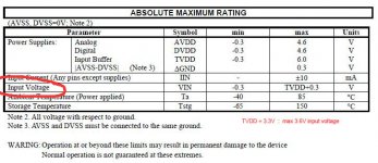
regarding the risks: AKM says it's not safe. Datasheet too, see 'absolute maximum ratings' section input voltage. The micro controller on this DAC is continuously probing the receiver IC (AK4113/AK4118), which is quite some stress if not the right voltage is used I think. PDN pin needs to be held high all the time, it's currently at the wrong voltage. I'm not sure if my DAC is performing better after the mod, the new chip needs to burn in, after that I can tell.
Weiliang better read this thread and make a better designed DAC, or I will...
terranigma: I agree, first I wasn't sure either, it's a bit confusing. But when you supply +5V to the TVDD pin, the chip can communicate with 5V logic, so then it's 5V logic tolerant indeed.
If you look at the DC-characteristics section of the datasheet, you see high and low level input voltage. High level can be max TVDD, so when TVDD = 3.3V, it may not exceed that voltage (which it does with pull-ups to 5V and 5V MCU)
Attachments

Last edited:
Hi guys,
What you guys are saying about the design being wrong resulting in the wrong voltage
regarding the tvcc----don't you think that problem should be addresed by Weiliang ?
Has anyone emailed Weiliang and asked him about this?
What you guys are saying about the design being wrong resulting in the wrong voltage
regarding the tvcc----don't you think that problem should be addresed by Weiliang ?
Has anyone emailed Weiliang and asked him about this?
NinoSimona:This is certainly cause for concern. I feel, at this point, that we need to hear what Weiliang has to say on the matter, so that we can be clear about what we have here. If you have email responses from AKM, then perhaps it would be the right time to present this in an email to Weiliang, for his comments.
I think I will do some measuring on my (4118) board, to see what's going on.
I think I will do some measuring on my (4118) board, to see what's going on.
Hi guys
I understand your concerns. I just encountered an error in the design of this DAC, why should I email the designer? I bought the DAC on *bay, not from Weiliang in person. He attached his name to the DAC design, I didn't notice any email address on the PCB,or did I overlook something?
Is he a member of this board also?
If he does, it's easy to invite him to comment on this subject, I've no problem with that.
Munkyone: Yes, check your version and report please😉
Last edited:
Hi NinoSimono,
I think that it is important to contact WeiLiang if there is a major design problem with his
dac. His email address is amp@diyhifishop.com
His first name is Jim.
I think that it is important to contact WeiLiang if there is a major design problem with his
dac. His email address is amp@diyhifishop.com
His first name is Jim.
Hi guys
I understand your concerns. I just encountered an error in the design of this DAC, why should I email the designer? I bought the DAC on *bay, not from Weiliang in person. He attached his name to the DAC design, I didn't notice any email address on the PCB,or did I overlook something?
Is he a member of this board also?
If he does, it's easy to invite him to comment on this subject, I've no problem with that.
Munkyone: Yes, check your version and report please😉
I will check my voltages in the next days, and report back. If I find the same problem on my version, I will certainly contact Weiliang about it, as I will want to understand his point of view.
Ok, it is just a cheap DAC board, with no expectations of 'best practice' design, but Weiliang does have some responsibility to at least answer any questions we may have regarding any potential errors discovered, particularly where any such errors may amount to a 'time-bomb' in the circuit. It is in Weiliang's interest to discuss this with us, both for the possibility of improving the products and to maintain customer confidence. The last thing he needs is bad vibes in the major audio forums.
However, for the money paid, the DAC's performance seems ok, and it is a fun DIY toy to experiment with 🙂
I totally agree with that. But those AKM chips are pretty advanced, I think they deserve a good designed PCB.However, for the money paid, the DAC's performance seems ok, and it is a fun DIY toy to experiment with 🙂
Design of this DAC could be improved for sure, resulting in better performance sound wise. Time for version 3 IMO.
I totally agree with that. But those AKM chips are pretty advanced, I think they deserve a good designed PCB.
Design of this DAC could be improved for sure, resulting in better performance sound wise. Time for version 3 IMO.
Cartainly there is potential in this dac chip. I agree it deserves a better PCB effort. I too, would like to see a v3, with better track layout, as discussed earlier in this thread A genuine attempt to get the most from the chips on a DIY budget. I am in.
I use modified emu-0404 usb with great results using the single ended output into two pairs of transistors. The transistors sound way better than the tubes in this application. I discovered the same thing using the tda1541 chip straight into transistors, then i/v, then buffer.
TVDD voltage affects SQ
To inform you guys what consequences the TVDD correction has for sound quality: Simply amazing, my DAC SQ has improved in every aspect!
I didn't expect it to be so influential, but truly, the sound has become much better, I didn't know this was possible: Dynamic Range++, Bass+, Detail+, Sound stage++, Authority+, amazing.
The current status of the receiver part of my DAC: AVDD has separate 3.3V low noise psu (as described in my earlier post), TVDD to +5V, replaced the AK4113 with a new one.
At the moment I am testing my DAC with the Arduino MCU: it works very well.
btw. I sent an email to the given address but didn't get a reply. I think the designer doesn't want to discuss the error.
You got all my attention! I have the Dual AK4399 with the 4118 receiver, is it the same procedure?
All you have to do is cut the trave and supply 3.3V using another reg? What is the current required?
Do
Last edited:
NinoSimona: Thanks for this. I am even more curious now 🙂 Just remains to figure out how to do this on the 4118 version board; it all looks very delicate around that chip 😱 perhaps I will get another chip, just in case!
What are you able to do better with the Arduino as MCU, as you have implemented it?
Also: Where on the board did you solder the 47u electrolytic to decouple the +5V
Jim (amp@diyhifishop.com) sometimes takes time to reply to messages. In my experience, he always replies. I pointed him to this thread a couple weeks ago and he replied positively, so he may already be reading this. I would have thought that for such a dramatic elevation in SQ, Weiliang would want to be all over this.
Last edited:
Hi Nino,
I went through AK4118A datasheet and it specify TVDD minimum power supply of DVDD = 3.3V and typical 5V, maybe I'm reading it wrong, but of course even if, it doesn't saying anything about possible improvement 😉
Hi Munkyone,
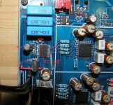
fortunately TVDD pin has pretty good access so there is enough space to cut traces and make other connection if necessary...
I went through AK4118A datasheet and it specify TVDD minimum power supply of DVDD = 3.3V and typical 5V, maybe I'm reading it wrong, but of course even if, it doesn't saying anything about possible improvement 😉
Hi Munkyone,
fortunately TVDD pin has pretty good access so there is enough space to cut traces and make other connection if necessary...
pinnocchio: Procedure is different. The version 2 PCB has 100n decoupling caps on the backside of the board. There must be a possibility though, just send me a high-res picture of the backside of the PCB.
Roughly the procedure is: cut the trace, connect it with a wire to a +5V track (of the same rectifier), and provide for decoupling close to the pin (10-47u electrolytic with 100n bypass). No extra regulator needed.
Munkyone: I can help you when I have a nice picture of the PCB backside.
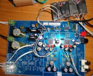
I use a better method with my Arduino MCU. The original MCU program is continuously checking a register of the AK4113 / AK4118 , using SPI. This stresses the chip, which isn't necessary at all: The receiver has the INT0 and INT1 pin, which change state when something happens, like changing the sampling frequency. This way, the MCU knows when to take action and when not, so it doesn't have to probe the register all the time (several times/sec!). Most of the time, when the DAC is locked to a signal and playing, the MCU can be held in sleep mode. The receiver chip then can do its core business, without being bothered all the time. Because this is audio, I think it's important to have as less as possible digital HF activity. For my MCU to work, I had to attach a wire to the INT0 pin. pictures follow
kukynas: Check out the table called 'DC characteristics', high level input voltage. The problem is not the voltage of TVDD alone. It can be 3.3V (the same as DVDD) as well. But only when the inputs (SPI clock, data in, cs, pdn) are connected to 3.3V logic (AK4113 and AK4118 are 3.3V devices). This is not the case in this design. Inputs are pulled up to +5V and a 5V MCU is used. In other words: the input buffer supply pin exists, because it provides a way to control the AK4113/AK4118 with 5V logic instead of 3.3V logic. In general you can't connect 5V logic to 3.3V device inputs, unless you use a level shifter.
Roughly the procedure is: cut the trace, connect it with a wire to a +5V track (of the same rectifier), and provide for decoupling close to the pin (10-47u electrolytic with 100n bypass). No extra regulator needed.
Munkyone: I can help you when I have a nice picture of the PCB backside.
I use a better method with my Arduino MCU. The original MCU program is continuously checking a register of the AK4113 / AK4118 , using SPI. This stresses the chip, which isn't necessary at all: The receiver has the INT0 and INT1 pin, which change state when something happens, like changing the sampling frequency. This way, the MCU knows when to take action and when not, so it doesn't have to probe the register all the time (several times/sec!). Most of the time, when the DAC is locked to a signal and playing, the MCU can be held in sleep mode. The receiver chip then can do its core business, without being bothered all the time. Because this is audio, I think it's important to have as less as possible digital HF activity. For my MCU to work, I had to attach a wire to the INT0 pin. pictures follow
kukynas: Check out the table called 'DC characteristics', high level input voltage. The problem is not the voltage of TVDD alone. It can be 3.3V (the same as DVDD) as well. But only when the inputs (SPI clock, data in, cs, pdn) are connected to 3.3V logic (AK4113 and AK4118 are 3.3V devices). This is not the case in this design. Inputs are pulled up to +5V and a 5V MCU is used. In other words: the input buffer supply pin exists, because it provides a way to control the AK4113/AK4118 with 5V logic instead of 3.3V logic. In general you can't connect 5V logic to 3.3V device inputs, unless you use a level shifter.
Last edited:
Hi Nino
At the end I don't understand if the same mod is raccomended even on board with ak4118 or not?
At the end I don't understand if the same mod is raccomended even on board with ak4118 or not?
Sorry, made a picture for you:Also: Where on the board did you solder the 47u electrolytic to decouple the +5V
Attachments
Hi keres,Hi Nino
At the end I don't understand if the same mod is raccomended even on board with ak4118 or not?
Yes, I would recommend it, but until now I/we didn't find the best way to do it on version2.
Also I must say, if you want to do this mod, cutting tracks etc. : it's at your own risk, and I can't give any guarantees you can achieve or hear the same improvements as I did, but I wouldn't recommend it if I wasn't sure about it. I also did mods to this DAC that didn't improve it significantly, which I didn't mention here because of that.
SW volume control?
Hi NinoSimona,
have you impelemented the software volume control already? Do you intend to implement remote control via IR in the MCU as well?
Watching eagerly your progress...😉
I use a better method with my Arduino MCU...
Hi NinoSimona,
have you impelemented the software volume control already? Do you intend to implement remote control via IR in the MCU as well?
Watching eagerly your progress...😉
My kit is running at last
Hi,
I recently replaced the dac chips of my kit (V1.1) and already did tvdd voltage fix. This fix is mandatory according to datasheet sections that Nino posted and his experiments confirms the problem. I cut the trace at 3.3V joint point and I tapped 5V at small regulator's input pin. I hadn't enough experience with non-fixed version thus I can't compare the sound difference that I attained so far.
I'm decided to go with transformer output. My transformers have dual primary windings (0.5+0.5:1) thus I was able to directly connect each differential section to transformers without needing any conversion.
My compliments about bass weakness entirely vanished with these AK4399's. The bass is so good. Maybe my separate analog supply for each dac chip helped the result I got. I built two separated Jbau's linear-phase/linear-impedance power supply for each chip's analog section. I used military grade axial tantalum capacitors around dac.
I tried to feed the chips via external Amanero USB/I2S adapter but the resulted sound was highly crippled. I think the software mode of chips require some extra directions in order to feed them externally. I'm not sure. According to the sound I get, AK4113 is a great receiver chip in my opinion. It seems I have to concentrate on improve power supply of receiver section rather trying to attach external i2s adapter.
Thanks for everyone sharing their experiments.
Attachments
Last edited:
Hi Nino,
you are right, again 😉
Hi keres,
it looks like it's needed...
Hi Monkyone
look at this picture, you can see TVDD pin marked, also traces, no need to cut any traces just take the first coil off and you can solder new wire in from your 5V supply, not sure if TVDD needs any additional filtering cap
you are right, again 😉
Hi keres,
it looks like it's needed...
Hi Monkyone
look at this picture, you can see TVDD pin marked, also traces, no need to cut any traces just take the first coil off and you can solder new wire in from your 5V supply, not sure if TVDD needs any additional filtering cap
- Status
- Not open for further replies.
- Home
- Source & Line
- Digital Line Level
- ebay:Weiliang Dual X2 AK4399 DAC with LCD