Hi Olaf, nice work I started pcb layout for A33 today. I was thinking to put offset correction section to right or left side of signal section. Your layout has given me some idea. Just little progress on pcb 😱.
Regards
Sonal
Hi, looks good. Feel free to use my layout. Only important to have a good running design at the end 🙂.
Regards Olaf
You also added 1000u+100n to each rail and increased 100u to 220u. Was this under advisement of Mile or did you just feel the circuit needed it?
Thanks, Terry
i have added 1000u + 100n after fuse, 100uF to 220uF is something i have found on olafk 's pcb,most of VAS part i copied from his A17 pcb and output stage is copied also from olafk 's APEX A20tef. other 100nF capacitors were added by me,they pro-long a life of el. capacitors they are connected in parallel with, and make their esr better (lower).
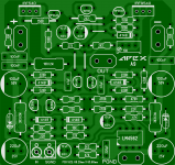
Final version of A9 pcb in sprint layout. Removed 3 jumpers and added 100nf bypass caps.🙂
Nice pcb,
Regards
i have added 1000u + 100n after fuse, 100uF to 220uF is something i have found on olafk 's pcb,most of VAS part i copied from his A17 pcb and output stage is copied also from olafk 's APEX A20tef. other 100nF capacitors were added by me,they pro-long a life of el. capacitors they are connected in parallel with, and make their esr better (lower).
So this is not actually the A23 but more of a combination of three amps? Do you have a schematic you can share? I only build these amps to learn. I don't need one more amp. I don't learn much if I am just blindly filling holes on a PCB.
Thanks, Terry
TEF or tripple emitor follower is (mostly) a kind of output stage,many amplifiers have tef in output. same goes for A23 and A20tef so the pcb in that part shares much similarities - that is why i used that part of olaf´s pcb.
we all have the same schematics,and the fact that i added a few capacitors doesn´ t change basic schematics at all. all i did is put a 100nF capacitor here and there(the goal was to impruve el-cap characteristics) and a 1000uF per rail just to get a bit more stabile rail current on the pcb.
we all have the same schematics,and the fact that i added a few capacitors doesn´ t change basic schematics at all. all i did is put a 100nF capacitor here and there(the goal was to impruve el-cap characteristics) and a 1000uF per rail just to get a bit more stabile rail current on the pcb.
I see, so no schematic to match this board? There is more than just some added caps. Looks like some sort of protection and maybe a clipping indicator? Like I said, I'm trying to learn. Stuffing parts is holes on a PCB is good soldering practice but not much more without seeing how the circuit works. Maybe if I just needed a good playing amp, but I have too many of those already.
Thanks, Terry
Thanks, Terry
This Pcb in pdf for transfer tonner metod?
Image - TinyPic - Free Image Hosting, Photo Sharing & Video Hosting
Mercy
Image - TinyPic - Free Image Hosting, Photo Sharing & Video Hosting
Mercy
Most users etch their PCB's self.Where can i buy these pcb's?
I see, so no schematic to match this board? There is more than just some added caps. Looks like some sort of protection and maybe a clipping indicator? Like I said, I'm trying to learn. Stuffing parts is holes on a PCB is good soldering practice but not much more without seeing how the circuit works. Maybe if I just needed a good playing amp, but I have too many of those already.
Thanks, Terry
Terry you can use one of these apex protection from Willy, its also my favorite. Pro from A23 pcb will connect to protection pcb.
Regards, Sonal
Attachments
You made my day!!!Hi Olaf, you have to rotate 2N5401 and 2N5551 180° they have EBC pinout.
Thank you.
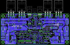
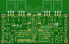
PCB rev 1.2 for A23
@olafk very good layout , nice compact design .....
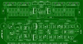
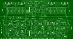
I think just a few members like my PCB rev 1.1 so I decided to try all in line OT for A23 so here it is .....but not tested !
Regards Alex
@olafk very good layout , nice compact design .....
I think just a few members like my PCB rev 1.1 so I decided to try all in line OT for A23 so here it is .....but not tested !
Regards Alex
Attachments
Last edited:
@olafk very good layout , nice compact design .....
I think just a few members like my PCB rev 1.1 so I decided to try all in line OT for A23 so here it is .....
Regards Alex
That's very cool ! I like your PCB's.
regards Olaf
picture: A33, some corrections
Thanks to Sonal Kunal.
Attachments
Hats off
Sonal, 44250, Alex, Olafk, Juan,
Very inspiring to see examples of your PCBs and how quickly you guys can come up with such excellent work..
and thanks again for the layout files - helps to actually learn hands on PCB layout instead of going straight to etching boards.
Apex, of course, is the Amplifier circuit machine beyond compare - as long as we keep building them he will keep cranking them out - the man never rests !
Thanks for the inspiration guys! It really helps to get the rest of us like me motivated to get off our butts.
Vic
I see, so no schematic to match this board? There is more than just some added caps. Looks like some sort of protection and maybe a clipping indicator? Like I said, I'm trying to learn. Stuffing parts is holes on a PCB is good soldering practice but not much more without seeing how the circuit works. Maybe if I just needed a good playing amp, but I have too many of those already.
Thanks, Terry
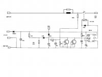
sorry, i wasn't thinking about that part of pcb: on the right it is "protect indicator" added from APEX-Zack NE555 protection and on the left there is clip indicator. that is added to a pcb but that does not affect the basic schematic of an amplifier or the way it works. i have had a free space on a pcb so that was the best way to use it,at the moment.
- Home
- Amplifiers
- Solid State
- 100W Ultimate Fidelity Amplifier