And what is VAS? I`m russian, do not understand
Voltage Amplification Stage.
Of course it is better in overall than 3EF, easy job for Q1, 2 as predrivers.
V3 should have exactly inverted voltage/temp curve as an uncompensated output stage on the main heatsink, excludind predrivers Q1, 2. Try to simm uncompensated output stage in operating temperature range and observe output bias according to V3. Inverted curve for V3 means proper compensation, keeping the bias constant (in theory).
V3 can be realised as discrete BJT temp sensor compensated Vbe multiplier or as NTC compensated IC shunt regulator.
All PNP outputs should be matched to each other only, the same with NPN, as they have to share the output current in equal proportion.
Thank you, LC.
I have experience with lateral mosfet only. What is best type for the mosfet? I choose IRFP240 dan IRFP9240 because I have the models 😀
I have experience with lateral mosfet only. What is best type for the mosfet? I choose IRFP240 dan IRFP9240 because I have the models 😀
Looks excellent to me. I will also experiment with simulation of this...
LC - thank you for pointing at it 😉
LC - thank you for pointing at it 😉
Looks excellent to me. I will also experiment with simulation of this...
LC - thank you for pointing at it 😉
I would like to see the result
If lateral mosfets are used as drivers temp compensation would be very easy, simple Vbe multiplier as temp sensor.Looks excellent to me. I will also experiment with simulation of this...
LC - thank you for pointing at it 😉
What is so special about BIGBT output stage:
- for six outputs per rail only three base currents flow through mosfet driver
- NPN-PNP base and therefore collector currents are completely equal
- very stable design no base-collector compensation capacitors needed
- very fast response especially if predrivers are used
- very easy to drive because of mosfet drive current isolation
- enormous output current capability
One good CFA should be proposed with this output stage.

If lateral mosfets are used as drivers temp compensation would be very easy, simple Vbe multiplier as temp sensor.

lateral have zero tempco
But lateral is very expensive 😡
Is there any lateral with high VDS (> 150V) and low ID (< 3A) and cheap?
Last edited:
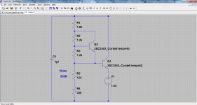
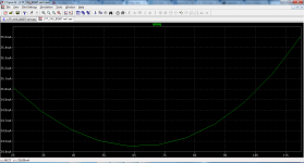
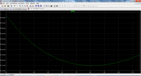
I sim VBE multiplier with lateral mosfet (2SK1058/2SJ162).
Lateral mosfet on separate heat sink and I assume the temperature is 60 degree Celsius. pre-driver and final transistor on same heat sink with VBE multiplier.
If pre-driver on separate heat sink, it slightly over compensated.
If all mount on same heat sink, it slightly under compensated.
Lateral mosfet on separate heat sink and I assume the temperature is 60 degree Celsius. pre-driver and final transistor on same heat sink with VBE multiplier.
If pre-driver on separate heat sink, it slightly over compensated.
If all mount on same heat sink, it slightly under compensated.
Attachments

Last edited:
Laterals should be on the main heatsink in the middle of outputs. Pre-driver on separate heatsink on PCB. Slightly over compensated tempco is OK for safety reasons, in practice this can be just right. 
Now one should bring to life this monster from 😀
😀
Now one should bring to life this monster from
😀Which one to use very much depends on implementation. Until now I've only used IRF610/9610 mosfets in BIGBT outputs, always without any issue. Lateral mosfets would certainly have some advantages like complete absence of secondary breakdown in SOA, negative tempco, low Ugs threshold voltage, no high frequency cross conduction, very robust and immune to oscillations. Sounds like I'm some kind of marketing manager but since I tested them a lot, there's practically no problems with them.
This case would be the first time to use lateral mosfets in BIGBT and I would definitely choose ALF08N20V and ALF08P20V. 🙂
This case would be the first time to use lateral mosfets in BIGBT and I would definitely choose ALF08N20V and ALF08P20V. 🙂
I sim BIGBT without EF, because I want gate-source capacitance be part of the compensation. I use push pull VAS, something like symasym but more complex.
The mosfet of BIGBT using IRFP240/IRFP9240 and 2SK1058/2SJ162.
The lateral mosfet give better THD dan slew rate. I will use lateral mosfet for BIGBT 😎
The mosfet of BIGBT using IRFP240/IRFP9240 and 2SK1058/2SJ162.
The lateral mosfet give better THD dan slew rate. I will use lateral mosfet for BIGBT 😎
OK, take five for this decision. 🙂
Please put ALFs inside, I can arrange some if you can't get them. 😉
Please put ALFs inside, I can arrange some if you can't get them. 😉
I'm currently working out a non switching Bryston-type OPS. Is the Bryston OPS topology patented?
Which one to use very much depends on implementation. Until now I've only used IRF610/9610 mosfets in BIGBT outputs, always without any issue. Lateral mosfets would certainly have some advantages like complete absence of secondary breakdown in SOA, negative tempco, low Ugs threshold voltage, no high frequency cross conduction, very robust and immune to oscillations. Sounds like I'm some kind of marketing manager but since I tested them a lot, there's practically no problems with them.
This case would be the first time to use lateral mosfets in BIGBT and I would definitely choose ALF08N20V and ALF08P20V. 🙂
thanks to your andwer
I already have hitachi but what most with the ALF?
This driver must be matched ?
Last edited:
- Status
- Not open for further replies.
- Home
- Amplifiers
- Solid State
- Simple Symetrical Amplifier