"Military grade" (bombproof) IPS's we shall have.
OS
I would face the mirror transistors in the same manner as the input pair. By mirroring both should be on the same temp to prevent discrepancy caused by temp difference. It costs nothing to project it once and the problem solved forever. Keep the tracks as short as possible, especially feedback ones.

Thanks Damir🙂OK the link is here, PS regulator with all needed protection.
http://www.diyaudio.com/forums/solid-state/182554-thermaltrak-tmc-amp-22.html#post3907062
Thanks Valery 🙂Here we go )
Just one thing... sorry, forgot to mention right away.
This PCB was made for mono-block. One channel.
For 7-channel design I use additional sub-PCB.
I can add second channel to it pretty easily. In couple of days.
This is difficult to make pcb.🙁
IF there was a ground plane on top of a double sided board, where would it be connected? To the power supply ground or signal ground or ???
I would face the mirror transistors in the same manner as the input pair. By mirroring both should be on the same temp to prevent discrepancy caused by temp difference. It costs nothing to project it once and the problem solved forever. Keep the tracks as short as possible, especially feedback ones.
But there already is a discrepancy ! These CM's are really current
multipliers.
The junctions of the 2 mirror devices will already have drastic differences.
If you look at the circuit , the VAS side of the CM magnifies at (680/150 =
@4.5 X or 1.65ma/7.2ma) ... then the LED's "bleed off" 2.5ma of the 7.2.
The led's Vf would also be a factor.
Swapping out models or just simulating one of the mirror devices has far
less effect than the main IP pair's electrical and thermal properties.
For a "blameless" like the badger , I have both the cascode and CM
facing the same way .... no drift.
Even as I like to go "face to face" with input pairs ....
This article - Heatsinks improve reliability
...shows that to-92's have 350c/w thermal resistance anyway , with
different Ic's , junction temp would be quite different. 🙁
PS - this will be single sided (toner transfer).
OS
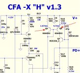
I await your interpretation of the CFA-XH. I think it will likely be the go-to IPS and if I order more OPSs I will make at least one IPS available (likely this one) at the same time.
I would be interested in CFA-XH IPS boards when and if you proceed.
Same here Jason if you make the CFA-XH count me in for a pair of boards to go with the output sections. I hope to see them perhaps this week, your check should be there about the same time I guess, you beat me by a couple of days I think.
Steven
Steven
It will come down to interest. I don't want to risk holding a quantity of boards if no one wants to build the design. The response to my initial order of OPS boards was a little softer than I expected which makes me a little gun-shy. Maybe having an official IPS on offer would make the difference.
In any event I look forward to seeing the CFA-XH develop, I think that is where my personal efforts will be going first.
In any event I look forward to seeing the CFA-XH develop, I think that is where my personal efforts will be going first.
Sorry teo hear that Jason.
I thought that all the ops boards had been spoken for and never thought that you had any extra's. I think in the end I will have to do some redesign, actually a combination of the input and output sections and adding a active xo before the input section. I.ll remove 3 of the 5 output pairs and make the entire board smaller in the end for my use. But I have other applications for myself where I will probably want to use all 5 output pairs down the road.
I thought that all the ops boards had been spoken for and never thought that you had any extra's. I think in the end I will have to do some redesign, actually a combination of the input and output sections and adding a active xo before the input section. I.ll remove 3 of the 5 output pairs and make the entire board smaller in the end for my use. But I have other applications for myself where I will probably want to use all 5 output pairs down the road.
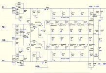
I got a pair of the Slew monster boards about 90% populated today. I need a few caps to finish. I used the MJL3281/1302 for the outputs but I used MJW3281/1302 for the drivers since they have a smaller footprint. Hopefully that will be OK. As I said earlier I plan to use Jason's CFA frontend first. I really want to give the Symasui ISP a go so hopefully someone will produce some Gerbers for that one.
blessings, Terry
blessings, Terry
VAS CM elaboration ...
Lazy cat got me thinkin' ....
I actually calculated the C/ per watt for each VAS current mirror.
The input device (Q5) just has .7V drop across it.
.00167A X .7V = .001169 watts 😱 This device has it "easy" ....
350C/w X .00117 = @ .4 Celsius junction temp. rise !
The main VAS mirror device , Q6 has a bit more work at 4.7ma Ic.
This will equate to about 5 Celsius junction rise.
So these mirror devices ARE running at different die temps - it might even
be better just to solder them in and NOT heat shrink them (couple).
The input pair in the "vssa" IPS is a different story.
Emitters are at +/- .6V and collectors are at rail - 2 volts.
Using the above math .... (I'll calculate for 60V rails) , ....
58+ .6 = 58.6V - 58.6 X .00167 = @ 100mW , which is a
35C junction temp rise. 😱
The IP pair does all the "heavy lifting" for this amp , coupling is essential
and one might even want to add small heatsink (or use larger devices)
The 1 W TO-92L's are lower C/W (80-100c/w) and to-126 devices
are 17c/w (ksa1381 for example).
Another factor is the CFA "current on demand" effect.
This is the "compromise" ... do we add another junction to cascode the
IP pair , or keep it stupid simple with just more robust devices ??
With the cascode we lose some speed , with the larger IP pair we gain
some Cob. BTW - we ALSO gain some cob with the added cascode.
Left as is , the circuit would best have a heatsinked or larger input
pair.
I used KSA1220A/ksc2690 as IP pair ... still have 12ppm !
PS - you most likely won't burn this circuit up with a to-92 pair ...
but the higher rail voltages of the "slewmaster" MUST be addressed.
OS
Attachments
Last edited:
Lazy cat got me thinkin' ....
So these mirror devices ARE running at different die temps - it might even
be better just to solder them in and NOT heat shrink them (couple).
On contrary, they have to be faced to the same temp. Take Q5 BE diode as a temp sensor for Q6. As they run different current ie. different power dissipation, Q5 is actually a temp sensor with just a fraction of power dissipation of Q6, acts as a bias servo for Q6, preventing Q6 collector current to rise in PTC manner. Q5 will simply regulate Q6 Ic according to temp rise and keep it in very tight Ic fluctuation, thus stabilizing VAS bias current.

IF there was a ground plane on top of a double sided board, where would it be connected? To the power supply ground or signal ground or ???
One plane is probably not an optimal layout for a double sided board, especially for a class B amplifier where different parts of the OPS reference different power supplies. Planes come into their own for a board with at least 4 layers, not needed for audio.
For a two layer board I think you need to consider the return path for each current and try to have the second side tracks mainly as return paths for the topside tracks.
Maybe easier to explain by example.
For instance the feedback connection between the OPS and IPS would overlay the quiet reference, usually earth (I haven't yet read Bruno Putzeys' article on this but differential should be similar.)
The collector and emitter traces for the OPS transistors would be another obvious candidate to pair, note that earth is not the reference here.
I have rarely seen this done well on a DIY amp, even otherwise impressive ones. I need to improve my test set-up to find out how much of an advance is possible.
Best wishes
David
Last edited:
I see your point ....On contrary, they have to be faced to the same temp. Take Q5 BE diode as a temp sensor for Q6. As they run different current ie. different power dissipation, Q5 is actually a temp sensor with just a fraction of power dissipation of Q6, acts as a bias servo for Q6, preventing Q6 collector current to rise in PTC manner. Q5 will simply regulate Q6 Ic according to temp rise and keep it in very tight Ic fluctuation, thus stabilizing VAS bias current.
even considering the lousy thermal thermal conduction of to-92 material,
Q5 will act as a Vbe for Q6. Sort of like some OPS's .. that use a to-92
for Vbe , as well.
I'll do it .. face to face (It will be harder 🙁 )
OS
It will be harder 🙁 )
It is worth it, always KISS-es, just not too many. 😎
I have a few questions about the caps.
How critical are the values? Are there some that have a range? Trying to learn something here. I look at C115-C124. They are listed as 22u. I see that they are basically in parallel. Is it critical that there be one per output or can it be taken care of with two or three if the totals add up? Are there other values that can be used?
Another question. I didn't have 68R for R113. Will 62R work? If so, does C114 change?
How critical is R103 at 1.8K? Can it be 2k or 1.5K? If so are there other changes that need to be made?
Thanks, Terry
Attachments
still4given:
CAVEAT:
I've built a lot of amps but none of the ones featured in this thread yet.
With that out of the way ...
C115-C119 and C120-C124 are physically close to the output devices; generally speaking having all four per rail is likely more important that having the total paralleled capacitance add up. I think you could get away with 10uF to 47uF if they fit physically (and electrically!).
Generally speaking, if I wasn't absolutely sure what the impacts are (is that an accurate assessment?), I would try hard to maintain any resistor values that impact output stage bias.
So ...
1. I would keep R113 at 68ohms if I didn't touch any other bias resistors.
Remember, you can make values by parallel and series connection of resistors too.
(and I wouldn't scale C114 based on a small change in R113).
2. I would keep R103 at 1.8Kohms. It is a bias or tempco resistor also so I would consider that value somewhat critical. I think 1.5K or 2K are too far away unless you adjust some other values, too.
You can use a trimpot or again use series or paralleled resistors to get values that you don't have as a single piece.
Hmmm ... just where is your bias trimpot anyway? I don't see one on the schematic anywhere.
If you have a bias pot, then you have a little flexibility to compensate for SOME of the resistor changes you are considering.
If you don't have a bias pot, well ...
good luck and post your results,
mlloyd1
- Home
- Amplifiers
- Solid State
- Slewmaster - CFA vs. VFA "Rumble"