Thanks for posting this up.
I've just redone my sims. For gain stepped from 10dB through 31.5 dB the -3dB CLG moves from ~575 kHz to 350 kHz with the ~575 kHz remaining essentially constant from 10 dB through 25 dB CLG which I would equate with the gain sweet spot often referred to in CFA application notes. This is with the bridge tie resistor set to 100 Ohms.
Those are really low BW's, in that case it requires a pretty detailed look at all the BW limiting issues. In my case input gm and Ccomp product is constant AND is the only BW determining factor so closed loop BW goes directly as closed loop gain.
Presumably, the THD20k @ 100W are SPICE world numbers.
Would you like to post the ASC so we can be astounded and amazed and maybe learn something? 🙂
asc file attached. I'm still working on it, with some fine tuning on the power supply, and some resistor value.
Sajti
Attachments
Hello Sajti,
Could you post a photo of your amp mentioned here if you have one.
Regards
Arthur
It's not yet ready, still under construction.
Sajti
Those are really low BW's, in that case it requires a pretty detailed look at all the BW limiting issues. In my case input gm and Ccomp product is constant AND is the only BW determining factor so closed loop BW goes directly as closed loop gain.
Here are the response curves.
The amplifier used in the sim is my sx-Amp with the non-inverting stage duplicated to provide inverting input buffer.
Attachments
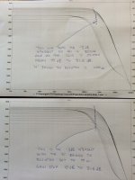
Here are the response curves.
The amplifier used in the sim is my sx-Amp with the non-inverting stage duplicated to provide inverting input buffer.
That's what I did , as well .. (mirrored the "NX") for the bridge.
The "bridge" is lower THD and is easier to "servo" , but compensation
is harder. As a trade-off , I prefer the attributes of the "true" CFA.
OS
Vintage 1985
Here is an amp I found in an article. DC to 140 kHz. 8A RMS at 2V compliance. It is intended for calibration laboratories to induce large currents in to very low impedance loads.
Would you call this a CFA?
Scaled up to 50 watts into 8R would be beautiful.
Schematic

Here is an amp I found in an article. DC to 140 kHz. 8A RMS at 2V compliance. It is intended for calibration laboratories to induce large currents in to very low impedance loads.
Would you call this a CFA?
Scaled up to 50 watts into 8R would be beautiful.
Schematic
Interesting. Rz is actually an output current sensor. Output current is converted to voltage with U2 op-amp and then sent to the inverting input of U1 via VFB.
I would put it into "current drive for loudspeakers" category.
For the scaled-up version I would rather put Rz below the output (between the speaker and the ground), making the signal more comfortable for U2.
I would put it into "current drive for loudspeakers" category.
For the scaled-up version I would rather put Rz below the output (between the speaker and the ground), making the signal more comfortable for U2.
That's what I did , as well .. (mirrored the "NX") for the bridge.
The "bridge" is lower THD and is easier to "servo" , but compensation
is harder. As a trade-off , I prefer the attributes of the "true" CFA.
OS
OS, I'm with you on this. For practical audio power amps I believe the Leach fully balanced VFA (and derivatives thereof incl folded cascode) and the standard CFA represent the best approaches.
Here is an amp I found in an article. DC to 140 kHz. 8A RMS at 2V compliance. It is intended for calibration laboratories to induce large currents in to very low impedance loads.
Would you call this a CFA?
Scaled up to 50 watts into 8R would be beautiful.
Schematic
View attachment 408911
Bob Carver used this in some of his so called magnet amplifiers decades ago. There is a write up on this on Rod Eliliot's audio pages for calculating FB parameters. This type of FB changes the output impedance of the amplifier. I've tried placing the sense resistor from ground to load series connected but the load reactance draws some serious attention to compensation of the amplifier. A series connected sense resistor tends to cause oscillation if the load is not purely resistive.
Here is an amp I found in an article. DC to 140 kHz. 8A RMS at 2V compliance. It is intended for calibration laboratories to induce large currents in to very low impedance loads.
Would you call this a CFA?
Scaled up to 50 watts into 8R would be beautiful.
Schematic
View attachment 408911
This is an original implementation of 'current feedback' before the advent of 'CFA' opamps changed the definition.
Jan
"debugged" TRUE CFA ...
Discussion is nice. But , in the end it must have a result.
(below) - is the output.
VERY well behaved , cheap , with <.5mv offset and 25ppm.
Anybody can build , and succeed the FIRST time.
All the CFA "weaknesses" are at least minimized (offset/PSRR).
OS
Discussion is nice. But , in the end it must have a result.
(below) - is the output.
VERY well behaved , cheap , with <.5mv offset and 25ppm.
Anybody can build , and succeed the FIRST time.
All the CFA "weaknesses" are at least minimized (offset/PSRR).
OS
Attachments
OS, can you post the ASC where you had trouble with the H-bridge?
Sure ... I know you will get it !!

I concede - not enough experience for this one . 😱
OS
Attachments
That's what I did , as well .. (mirrored the "NX") for the bridge.
The "bridge" is lower THD and is easier to "servo" , but compensation
is harder. As a trade-off , I prefer the attributes of the "true" CFA.
OS
I put the H bridge version into the simulator, and it gives nice 1ppm at 1kHz, and about 5ppm az 20kHz. Simulated DC offset was 11mV with separated DC feedback loop, and no offset compensation.
Sajti
OS, I didn't find anything wrong with the input stage, but I did find that a 100R//820p network was needed for the drivers' bases. So, it was a problem in the output stage as far as I can tell. Also, you need to add Rdm2 to the LTP buffer emitters, so it has a workable bias. Until I did that the OPS and VAS had almost no bias.
Re offset/bias.
Be warned that if the degeneration voltage applied to the front end devices is too low, you will get problems.
About 60 (30 sets) individual nx-Amp boards have been sold and I've had 4 complaints where the output offset could not be dialed out and or the second stage bias was wrong (this is tested by measuring the voltage across the 1 k collector load resistors of the diamond buffer output stage).
In the original design, I used 15 ohm resistors and 1 mA standing currents to generate 15 mV degeneration.
This is not enough to deal with the normal Vbe spreads, and you can end up with some amps where the diamond output stage is starved of current and/or the aforementioned offset issues. HFE matching by the way will NOT solve the problem - it's a delta Vbe issue between the transistors.
To overcome this, I raised the degen voltage to 150 mV and 120 mV for the buffer and level shifter respectively by changing the 15 Ohm resistors for 150 Ohms and 110 Ohms.
The offset adjustment is now smooth and gives +-500 mV range, and the standing current variation spread from unit to unit will be much narrower.
There is an errata sheet posted up in my website, and I've added it to the sx & nx amp thread.
To be sure, if you use complements for the input stage (so BC557C and BC547C for example) and a cascode, the problem will be much reduced, but I would still encourage the use of higher degeneration voltages on diamond buffers. In the nx-Amp, I've used a 45 V Vce BC5x7C for the buffer, and 65 V Vce rated BC5x6B for the level shifter because I did not want to use a cascode and it seems this also contributed to the now solved problem.
On one full builds, problems like this would likely not be caught - you'd build and get away with it as was my case where I built 2 protos, and then two final boards with no issue, only discovering the problem after building a further two. When you produce many exemplars, spread issues like this will raise their heads.
I spent a few hours testing and pushing the two new boards this week end and am extremely happy with the results. Square wave 100 kHz at near full power and rise fall times of c 700 ns - so no change to the performance.
Last edited:
The thermal and bias issues can be designed out, so only the Vbe spread problem remains. I think sticking to major modern manufacturers for devices will control this very well; I've measured BCxxx transistors from Fairchild and OnSemi to be within 1mV.
Just ran into the same issue - had to tell builders to "up" the IP diamond Re's
to 39R ... I run 1.8-2ma at ip (70+mv Re). 🙁
Had overshoot and the servo worked too hard to correct offset.
Now, having both fully adjustable CCS's and the servo , I can
advise for even higher values for higher gain IP pairs.
My builders are throwing everything in the "junkbox" into my amps 😱 .
The amount of current feedback also affects the ease of mitigating
offset. So , One must compromise between slew , how large and how hot
your FB resistors have to be , and the ease in which the servo can correct
all this. (or , in your case ... the passive offset trim).
PS - I have also advised to match the IP P/N with a DMM , at least get "close".
OS
To clarify, I was meaning 1mV matching between same parts, not complimentary.
With the transistors I got, matching complimentary devices would be hard because you couldn't do better than 1mV or so from normal, since the individual device spreads are so low. And if you DID manage to find one transistor in a large batch that had significantly different Vbe, how do we know that device wasn't damaged by ESD or is a dud?
With the transistors I got, matching complimentary devices would be hard because you couldn't do better than 1mV or so from normal, since the individual device spreads are so low. And if you DID manage to find one transistor in a large batch that had significantly different Vbe, how do we know that device wasn't damaged by ESD or is a dud?
Last edited:
OS, I didn't find anything wrong with the input stage, but I did find that a 100R//820p network was needed for the drivers' bases. So, it was a problem in the output stage as far as I can tell. Also, you need to add Rdm2 to the LTP buffer emitters, so it has a workable bias. Until I did that the OPS and VAS had almost no bias.
I put that network on the "doubleD" , and you are right on.
But , on my other amps .. the driver network "rings" (overshoots).
Interaction between just some IPS's - and the OPS ? 😕
I did design ahead - pads for a driver network are an option on
JK's slewmaster OPS. 🙂
OS
- Home
- Amplifiers
- Solid State
- CFA Topology Audio Amplifiers