I have been using HCl and H2O2 for really nice fast etching, and as you use it you gradually get the CuCl etchant as a result. My current recipe is pretty fast without being too noxious (it does off-gas some so do this outside or at least in a well ventilated area anyhow). I'm using:
2 parts water
2 parts HCl (~38% 'pool acid', this fumes)
1 part 30% H2O2 (this can be bought from beauty supply stores as hair bleach)
Room temperature gave me about a 120 second etch of 1oz copper clad.
Don't do it. I have it used 20 years ago for some time but it is too dangerous for your health. This etching procedure (which is indeed very fast) produces a very harmful substance:
- chlorine gas
While being financially marginal , I found the web article on HCL/H2O2 etching
and thought it VERY helpful and simple.
I did get a few whiffs of the outcome , and became quite fearful of the
effects. Even waiting for windy days (staying downwind)
, preheating the components (in hot water) to optimum "burn" temp. ...
I avoided any further exposure ... but I don't like close calls. HCL lung burns
and CL2 toxicity are true risks that a few more dollars could minimize.
A link to many alternatives ....
Which etching solution is most safe? - All About Circuits Forum
PS - the muriatic/peroxide is so widely used and linked to on google ...
the others are rather hard to find 😕 .
OS
Maybe you are wealthy enough to have an indoor pool 😉. I got a raised eyebrow when I asked for it recently too. Also, pool, spa and HW stores generally call it muriatic acid (it is HCl by an older name) just in case you aren't aware of that.
My printer turned out not to work with this product, but it released the toner very well. I think with one of the low melting point toners used by HP it could give good results. They also recommend a specific laminator for the transfer. I might give this a shot again in the future.
PCB Fab-in-a-Box
I did fab in a box with an Iron and failed , tried it with a cheap laminator .. it
worked a few times and then the machine "de- laminated" .
The best I've seen on the web is a E-waste copy machine fuser assembly removed , tweaked for pcb tolerances and toner temp with a custom
heater regulator circuit.
This would do nice .1mm or better digital SMD transfers !!
-- Toner Transfer Fuser | The Steampunk Workshop
Thats DIY !! 🙂
OS
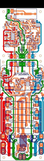
Here is the newest 3 -pair ... there is a typo (that orphan resistor) in that color
layout.
Schema/copper/screen - normal and reverse polarity to facilitate IPS facing
away or to OPS.
Also , once we build a fully functional OPS w/ no "bugs" and get a good IPS
to "sing" on it . The "sky is the limit" within the OPS's capability. 😎
PS - If you printed the "typo" , board is still fully electrically sound....
observe "typo" to make sure it does not bridge anything (it might not be there
on the copper file).
"New" is the same layout with "housekeeping" (same schema).
OS
Attachments

You read my mind uncle OS,...Here is the newest 3 -pair ...
Schema/copper/screen - normal and reverse polarity to facilitate IPS facing
away or to OPS.
PS - If you printed the "typo" , board is still fully electrically sound....
observe "typo" to make sure it does not bridge anything (it might not be there
on the copper file).
"New" is the same layout with "housekeeping" (same schema).
OS
so the R111 & R112 is 22 ohm 🙂
I thought it was jumpers.
I made slimmer board for the OPS,
make it a bit different from yours because
the parts available here a bit different too.
kcs3503
I made slimmer board for the OPS,
make it a bit different from yours because
the parts available here a bit different too.
Dissapointed KSC3503 not available in my city
I made slimmer board for the OPS,
make it a bit different from yours because
the parts available here a bit different too.
Dissapointed KSC3503 not available in my city
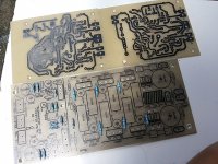
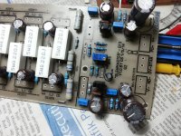
My progress so far...
Nice "industrial" looking OPS ! It looks like it means business ...
PS - you do have that "glitch" (the orphan resistor near the IPS euroterms)..
make sure its pad do not touch anything - you could "erase it".
OS
My progress so far...
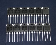
Hi, Naf where do you buy the output transistor? I have trouble to get them.
Nice "industrial" looking OPS ! It looks like it means business ...
PS - you do have that "glitch" (the orphan resistor near the IPS euroterms)..
make sure its pad do not touch anything - you could "erase it".
OS
Thank you Uncle OS,
Here the bottom, orphan resistor clearly safe not touch any pad. So i don't have to install this resistor right?
Attachments
Hi, Naf where do you buy the output transistor? I have trouble to get them.
I have a couple i've bought one year ago... when i start to build my Badger Amp.
Hi, Naf where do you buy the output transistor? I have trouble to get them.
I have a couple i've bought one year ago... when i start to build my Badger Amp.
I'm still collecting the parts, here are the NJW
so it is rare now in our country 😀
I'm lucky that I also bought them last year
Can we changed the OPS transistor with the bigger package?
like the popular TO-264 or even TO-3, I have a lot MT-200 too 🙂 big fans of them
so that orphan resistor does't do anything, I thought it will be use for something special, hehe... 😀Thank you Uncle OS,
Here the bottom, orphan resistor clearly safe not touch any pad. So i don't have to install this resistor right?
keep your spirit mas Naf... your the lucky one to solder it first 🙂
Attachments
Last edited:
While being financially marginal , I found the web article on HCL/H2O2 etching
and thought it VERY helpful and simple.
I did get a few whiffs of the outcome , and became quite fearful of the
effects. Even waiting for windy days (staying downwind)
, preheating the components (in hot water) to optimum "burn" temp. ...
I avoided any further exposure ... but I don't like close calls. HCL lung burns
and CL2 toxicity are true risks that a few more dollars could minimize.
A link to many alternatives ....
Which etching solution is most safe? - All About Circuits Forum
PS - the muriatic/peroxide is so widely used and linked to on google ...
the others are rather hard to find 😕 .
OS
The chemistry of copper unfortunately must always lead to emission of toxic gases when the copper is etched. least dangerous for the diy is ammonium persulfate. H2O2 + HCL is exotherm.
The "galvanic" method has a huge advantage : you need a tiny amount of HCL in water and a current source. The "etched" copper lands on for ex a graphite electrode and the diy has no problems how to get rid of poisonous
copper chloride copper sulfate...he has pure copper.

Almost at the next step ...
When you get to placing the output transistors , the OPS can be tested
(in isolation) by putting 15K resistors between the (V+/PD+) and (V-/ND-)
euroterminal connections.
This will emulate a 4.5mA IPS hooked to the output stage. You can adjust
the "bias" to around 200R to see the 65-75ma at any of the .22R RE's.
You can also test the outputs of the cap multipliers. They should be rail -
about 2V... apiece.
Temporarily Heatsink whatever outputs you solder in. With a DMM, you will
also be able to see the main Vbe's thermal response to a lighter or other
heat source. The main Vbe is UNDERNEATH the PCB ... you screw it down
through the large hole near the drivers.
The "small Vbe" is attached to
the plate of aluminum/copper that the main drivers are thermally bonded to.
OS
Enough for today...
When you get to placing the output transistors , the OPS can be tested
(in isolation) by putting 15K resistors between the (V+/PD+) and (V-/ND-)
euroterminal connections.
This will emulate a 4.5mA IPS hooked to the output stage. You can adjust
the "bias" to around 200R to see the 65-75ma at any of the .22R RE's.
You can also test the outputs of the cap multipliers. They should be rail -
about 2V... apiece.
Temporarily Heatsink whatever outputs you solder in. With a DMM, you will
also be able to see the main Vbe's thermal response to a lighter or other
heat source. The main Vbe is UNDERNEATH the PCB ... you screw it down
through the large hole near the drivers.
The "small Vbe" is attached to
the plate of aluminum/copper that the main drivers are thermally bonded to.
OS
I'm still collecting the parts, here are the NJW
so it is rare now in our country 😀
I'm lucky that I also bought them last year
Can we changed the OPS transistor with the bigger package?
like the popular TO-264 or even TO-3, I have a lot MT-200 too 🙂 big fans of them
so that orphan resistor does't do anything, I thought it will be use for something special, hehe... 😀
keep your spirit mas Naf... your the lucky one to solder it first 🙂
You can also use the 5200/1943 pair .... any 30mhz Ft output pair. The
21193/94 will also work. MT-200 is just a tad too large. 🙁
The optimum is slow predrivers/fast drivers/slow outputs. (slow/fast/fast) is
also acceptable.
OS
Thank you very much Os, i'll follow your guide and ask if there is something i don't understand. 😎When you get to placing the output transistors , the OPS can be tested
(in isolation) by putting 15K resistors between the (V+/PD+) and (V-/ND-)
euroterminal connections.
This will emulate a 4.5mA IPS hooked to the output stage. You can adjust
the "bias" to around 200R to see the 65-75ma at any of the .22R RE's.
You can also test the outputs of the cap multipliers. They should be rail -
about 2V... apiece.
Temporarily Heatsink whatever outputs you solder in. With a DMM, you will
also be able to see the main Vbe's thermal response to a lighter or other
heat source. The main Vbe is UNDERNEATH the PCB ... you screw it down
through the large hole near the drivers.
The "small Vbe" is attached to
the plate of aluminum/copper that the main drivers are thermally bonded to.
OS
The optimum is slow predrivers/fast drivers/slow outputs. (slow/fast/fast) is
also acceptable.
OS
Interesting! I'm gonna search for more info concerning this matter.
Interesting! I'm gonna search for more info concerning this matter.
Bob Cordell ... in the "troubles with triples" thread , hinted at this.
I took it as good advice , but had to further "play".
Using a real low Cob fast predriver 1381/3503 resulted in the most unstable triple.
It could be made to run on some IPS's by including it in a highly compensated FB loop.
My HK uses 50mhz predrivers , 70mhz sa1837/sc4793 (toshiba) , and slower
sanken OP's. Any fast predrivers I've seen on OEM's shunt C-B to make the 2'nd
stage (main drivers) fastest.
In simulation MJE340/350 or mpsa42/92 as predriver seem to make for EF2 like stability
while attaching all these varied input stages.
Of these combo's for BJT's ... mpsa92/42 - mje15032/33 - MJL21193/4
makes for the perfect current magnifier.
My mje340/350 - njw0281/0302 - njw0281/0302 is also super stable.
OS
- Home
- Amplifiers
- Solid State
- Slewmaster - CFA vs. VFA "Rumble"