So, what is your desing philosophy ?
I am not a philosopher. The simplest answer is I have made the amp using parts I had by hand. Then some circumstances made me put any works aside. Good thing is a discussion about E180F proper op point which I am going to use in the next incarnation - with DN2540s. Anyway, thanks
...Good thing is a discussion about E180F proper op point which I am going to use in the next incarnation - with DN2540s. Anyway, thanks
The proper operation with a CCS must be studied by testing.
From tube data sheets can be found only a slight idea about it.
In general the proper operation point is what produces lowest THD at the required signal level.
The only way to find this is to use some sort of distortion analyzer.
I am not a philosopher. The simplest answer is I have made the amp using parts I had by hand. Then some circumstances made me put any works aside. Good thing is a discussion about E180F proper op point which I am going to use in the next incarnation - with DN2540s. Anyway, thanks
Yagoolar, I'm sorry but you do not need to be a philosopher to get much more from your driver.
Remove R14, R13 and R15, get 330V at 68 ohm resistor. Set current 11-12mA at CCS, and that's all. You'll be in.
Yagoolar, I'm sorry but you do not need to be a philosopher to get much more from your driver.
Remove R14, R13 and R15, get 330V at 68 ohm resistor. Set current 11-12mA at CCS, and that's all. You'll be in.
Rajko,
Don't be sorry - the question was about design philosophy. I am quite aware of lack of perfection in my compilations, which are not *my* designs.
Your recommendations are valid as far as an HV transistor has higher power dissipation. Da capo al fine - CCS needs to be redesigned.
This is so far the most linear high level driver circuit I have built, (not only simulated).
With Soviet 6J11P-E and biased to: +Ub = 350 V, Ua = 170 V, Ik = 8,3 mA, Rk (R15) = 390 ohms, THD = 0,05 % @ 200 Vpp.
With 6J9P the THD is a bit higher.
An externally hosted image should be here but it was not working when we last tested it.
With Soviet 6J11P-E and biased to: +Ub = 350 V, Ua = 170 V, Ik = 8,3 mA, Rk (R15) = 390 ohms, THD = 0,05 % @ 200 Vpp.
With 6J9P the THD is a bit higher.
This is so far the most linear high level driver circuit I have built, (not only simulated).
An externally hosted image should be here but it was not working when we last tested it.
With Soviet 6J11P-E and biased to: +Ub = 350 V, Ua = 170 V, Ik = 8,3 mA, Rk (R15) = 390 ohms, THD = 0,05 % @ 200 Vpp.
With 6J9P the THD is a bit higher.
Is C4 really 22uF?
The gain, low frequency response and phase shift at low end is not changed even if C4 is fully removed.
The reason is very high anode impedance due to active anode load.
The reason is very high anode impedance due to active anode load.
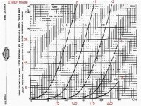
Mullard E180F triode curves
I see that today is possible to upload file.
On JA2DHC site is an excellent spice model for E180F (6688), Nakobayashi method.
Attachments
I see that today is possible to upload file.
On JA2DHC site is an excellent spice model for E180F (6688), Nakobayashi method.
Rajko,
Do you mean those ones? Tube Models for TINA
Yes. For use in LTspice you need convert all ^ to **. This applies to all Ayumi`s models.
Thanks to JA2DHC
* Generic pentode model: E180F
* Copyright 2003--2008 by Ayumi Nakabayashi, All rights reserved.
* Version 3.10, Generated on Wed Jun 24 22:54:24 2009
* Plate
* | Screen Grid
* | | Control Grid
* | | | Cathode
* | | | |
.SUBCKT E180F A S G K
.PARAM X1=-0.59576533 X2=0.0094827837 X3=-0.8531559
.PARAM X4=0.63744183 X5=38.233306 X6=2.3531559
.PARAM X7=0.01902963 X8=59.979286 X9=0.011758543
.PARAM Y1=0.0095148149 Y2=0.80517343 Y3=0.19482657
.PARAM Y4=0.009992698 EA=2523.93
BK IK 0 V=U(V(G,K)+X1)*X7*URAMP(V(G,K)+X1+URAMP(V(S,K))/X8)**1.5+(1-U(V(G,K)+X1))*X9*(X2*URAMP(V(S,K)))**X3*(X4*URAMP(V(G,K)+X1+URAMP(V(S,K))/X5))**X6
BL IL 0 V=(V(IK)-Y1*URAMP(V(G,K))**1.5*(URAMP(V(G,K))/(URAMP(V(A,K))+URAMP(V(G,K)))*1.2+.4))*(1-.4*(EXP(-URAMP(V(A,K))/URAMP(V(S,K))*15)-EXP(-15)))
BM IM 0 V=V(IL)*(URAMP(V(A,K))+EA)/(URAMP(V(S,K))+EA)-URAMP(V(IL)*(URAMP(V(A,K))+EA)/(URAMP(V(S,K))+EA)-(Y4*(URAMP(V(A,K))+URAMP(URAMP(V(S,K))-URAMP(V(A,K))))**1.5))
BA A K I=URAMP(Y4*URAMP(V(A,K))**1.5-URAMP(Y4*URAMP(V(A,K))**1.5-V(IM)+V(IL)*(Y2*(1-URAMP(V(A,K))/(URAMP(V(A,K))+10))**1.5+Y3)))+1E-10*V(A,K)
BS S K I=URAMP(V(IM)-URAMP(Y4*URAMP(V(A,K))**1.5-URAMP(Y4*URAMP(V(A,K))**1.5-V(IM)+V(IL)*(Y2*(1-URAMP(V(A,K))/(URAMP(V(A,K))+10))**1.5+Y3))))
BG G K I=Y1*URAMP(V(G,K))**1.5*(URAMP(V(G,K))/(URAMP(V(A,K))+URAMP(V(G,K)))*1.2+.4)
* CAPS
CGA G A 0.03p
CGK G K 5.1p
CGS G S 3.4p
CAK A K 3.5p
.ENDS
** Generic triode model: E180F_T
* Copyright 2003--2008 by Ayumi Nakabayashi, All rights reserved.
* Version 3.10, Generated on Wed Jun 24 22:55:42 2009
* Plate
* | Grid
* | | Cathode
* | | |
.SUBCKT E180F_T A G K
.PARAM X1=-0.59576533 X2=0.0094827837 X3=-0.8531559.
.PARAM X4=0.63744183 X5=38.233306 X6=2.3531559
.PARAM X7=0.01902963 X8=59.979286 X9=0.011758543
.PARAM Y1=0.0095148149 Y2=0.009992698
BK IK 0 V=U(V(G,K)+X1)*X7*URAMP(V(G,K)+X1+URAMP(V(A,K))/X8)**1.5+(1-U(V(G,K)+X1))*X9*(X2*URAMP(V(A,K)))**X3*(X4*URAMP(V(G,K)+X1+URAMP(V(A,K))/X5))**X6
BA A K I=URAMP((Y2*URAMP(V(A,K))**1.5)-URAMP((Y2*URAMP(V(A,K))**1.5)-V(IK)+Y1*URAMP(V(G,K))**1.5*(URAMP(V(G,K))/(URAMP(V(A,K))+URAMP(V(G,K)))*1.2+.4)))+1E-10*V(A,K)
BG G K I=Y1*URAMP(V(G,K))**1.5*(URAMP(V(G,K))/(URAMP(V(A,K))+URAMP(V(G,K)))*1.2+.4)
* CAPS
CGA G A 3.43p
CGK G K 5.1p
CAK A K 3.5p
.ENDS
The gain, low frequency response and phase shift at low end is not changed even if C4 is fully removed.
The reason is very high anode impedance due to active anode load.
Someone correct me if I am wrong: with output connected to source of the mosfet output impedance provided gm*R1 >>1 is 1/gm, or approx. 1 ohm for IRF820.
High output impedance would be if the output were connected to the anode.
Too optimistic
This is a value I measured from actual circuit, not LTspice simulation.
If you have 6J11P-E tubes, try and see.
Someone correct me if I am wrong: with output connected to source of the mosfet output impedance provided gm*R1 >>1 is 1/gm, or approx. 1 ohm for IRF820.
High output impedance would be if the output were connected to the anode.
Yes.
This is a value I measured from actual circuit, not LTspice simulation.
If you have 6J11P-E tubes, try and see.
Too optimistic, as I said.
Calculate k1, k2, k3... from curves for E180F_triode, it's easy.
You will see, for current about 8 mA, total harmonic distortion will be >2%
I have built such amplifier, as I said:
- 6J11P_IRF820 mu-follower having 0,05 % @ 200 Vpp (about 70 Vrms) with 350 V supply voltage.
Build one, fine tune and measure, it's easy.
I have said nothing about E180F.
- 6J11P_IRF820 mu-follower having 0,05 % @ 200 Vpp (about 70 Vrms) with 350 V supply voltage.
Build one, fine tune and measure, it's easy.
I have said nothing about E180F.
I have built such amplifier, as I said:
- 6J11P_IRF820 mu-follower having 0,05 % @ 200 Vpp (about 70 Vrms) with 350 V supply voltage.
Build one, fine tune and measure, it's easy.
I have said nothing about E180F.
Constant voltage source (gyrator) will somewhat reduce THD but not more than 20-25%.
In any case, I prefer CCS over CVS for driver stage.
I'm not a fan of mu-follower, except as output in some RIAA preamps.
6J9PE is similar to E180F. Better?? Not!
As to the triode model of E180F_T posted above - beware, there is "." (dot) is added after X3 value. You need to remove it. See below:
--------------------------------------------------------|
.SUBCKT E180F_T A G K
.PARAM X1=-0.59576533 X2=0.0094827837 X3=-0.8531559.
It should read
.SUBCKT E180F_T A G K
.PARAM X1=-0.59576533 X2=0.0094827837 X3=-0.8531559
--------------------------------------------------------|
.SUBCKT E180F_T A G K
.PARAM X1=-0.59576533 X2=0.0094827837 X3=-0.8531559.
It should read
.SUBCKT E180F_T A G K
.PARAM X1=-0.59576533 X2=0.0094827837 X3=-0.8531559
Last edited:
- Status
- Not open for further replies.
- Home
- Amplifiers
- Tubes / Valves
- E180F V EF184