Nope. All from one lot. I did get your PM, thank you. I realize now the person who I have been having trouble with is Ravid. He sent me an email through the system and I cannot respond, as it is blocked.
I have not spent to much time but only one led is lighting up, one next bias pot not lighting and bias voltage wrong. Checked LED its good, any thoughts? I have not checked the other board yet (no r100 installed yet).
Bill
Bill
Now they bias up and offset nicely, any other test I can perform before installing the output devices?
Bill
Bill
Don't need to close eyes, I have a variac to bring them up slowly. On the Alephs when you bring them up slowly the would have a lot of offset until full power. I would think these would be a lot tamer as they are not using a constant current source.
Bill
Bill
Closing eyes is more exciting
Stooping a bit to the side with your shoulders close to your ears also helps some times
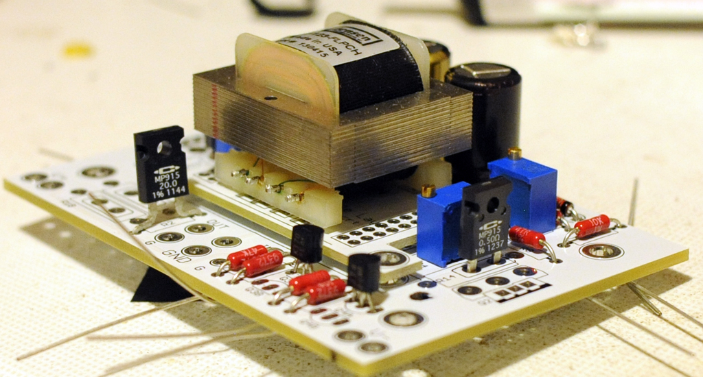
I just finished dry fitting the parts.
It seems that R13 and R14 are 0.5R caddocks (for IRFs), R2 is a 20R Caddock, a 9.1V zener for the led reference.
Are these correct? Also, what is the polarity mark on the Jensens? Or should I just align the letters and then the dot on the boards?
I m also a bit concerned about the zener polarity. Do they look ok?
Also about the FE, with 10mA jfets, I guess we only populate Q3A qnd Q4A right?
I also do not have an R1. Justin did you forget that one or it would not be included in the GB?
Thanks again for a nice package.
Attachments
Everything is correct exept for Jfet. the pinout on the Jensen will help locate it properly. Pin 1 is the only one with a smaller offset. You should have two R1's.
Also see post #41 for link to Jensen pdf, and post #144 for a nice pic of proper daughter card orientation.
Some good info in Tea's F6 blog about FE considerations. My understanding is you're good to go with one pair 10mA jfet and R11/R12 as supplied by buzz.
BK
Some good info in Tea's F6 blog about FE considerations. My understanding is you're good to go with one pair 10mA jfet and R11/R12 as supplied by buzz.
BK
Justin's mention of the offset makes perfect sense.
Basically you cannot solder the Jensen on the daughterboard in a wrong way unless you force it and bend the pins significantly.
You just have to be careful to follow the dots on the boards to attach the daughterboard
Basically you cannot solder the Jensen on the daughterboard in a wrong way unless you force it and bend the pins significantly.
You just have to be careful to follow the dots on the boards to attach the daughterboard
Hi all
got the parts thanks Buzz!!
few questions
I,m building the f6 buffered using the original schematic on the firstwatt site
and I need to clarify a few things
1, the f6 buffered schematic above does not have r11/12 I suspect these are for jft degeneration ,do I use them ? if so what goes there (I have 4 x 10r left from buzz,s kit after populating everything as per the above schematic )
2, what way do the led install ,one of the solder pads is square the other is round(teas boards)
3, what are the diodes for in the kit ,the f6 buffered schematic does not show any
4, do I have to install p3 /p4, I just want to build as per nelsons original circuit which does not use these
rgds Sheafer
Could you take a closer pic of those zeners,couse I got a resistor there instead,or maybee that will work as well?It seems that R13 and R14 are 0.5R caddocks (for IRFs), R2 is a 20R Caddock, a 9.1V zener for the led reference.
The Zener's were included for those folks who would be using the IRF outputs. It give you a larger voltage to divide down with the pot for the gate of the mosfet.
The Led's have one long leg. That leg is the anode of the LED.
You will have to post the schematic you are talking about for me to know how to advise. There were several put out in the article
The Led's have one long leg. That leg is the anode of the LED.
You will have to post the schematic you are talking about for me to know how to advise. There were several put out in the article
HI Buzz
I just noticed the 'f6 variable 2nd' schematic which matches the board and parts so I guess that is what I will put together
re the zeners , im using r100 semis so does that mean im just to install both led,s ?
Sheafer
I just noticed the 'f6 variable 2nd' schematic which matches the board and parts so I guess that is what I will put together
re the zeners , im using r100 semis so does that mean im just to install both led,s ?
Sheafer
- Status
- Not open for further replies.
- Home
- Group Buys
- GB for F6 Convertible Clone boards