Just wait some more. There will be a second version.... The SPDIF version will definitely come without the U.FL connectors as the DAC will be better without them. The SPDIF version will be as pure as I can make it without any bells and whistles. I am not regretting that. The U.FL connector is a lousy connector mechanically (but it is good electrically).
We know some of you have plans with our DAC. You won't be disappointed. It might be that you get a surprise for the long waiting. I can not tell anymore as I signed an NDA with Subbu 😉
Thank you!!
Patience can be a virtue!
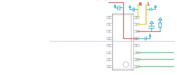
Maybe a hybrid-pad layout can be possible around the I2S termination resistor pads ?
If u.fl input is needed, so no termination resistors are fitted, so termination resistor pads (for the WM8804 side) can be modified pad design for u.fl gnd/smt resistor ?
For me, I do not need u.fl but I hope for common board design, not 3 different.
For spdif input, any pulse transformer ?
If u.fl input is needed, so no termination resistors are fitted, so termination resistor pads (for the WM8804 side) can be modified pad design for u.fl gnd/smt resistor ?
For me, I do not need u.fl but I hope for common board design, not 3 different.
For spdif input, any pulse transformer ?
Different boards, no possibility for U.FL on the SPDIF version, also no pulse transformer. After years of trying those I found none work better than no transformer at all (provided that the source has one). I haven't seen many sources without transformer and if they hadn't it were sources that I wouldn't use for serious audio.
Last edited:
Thank you for those awaited informations Jean Paul 
I've tested my board with I2S only, SPDIF part unpopulated, except one PSU line required for USB/isolator (3.3v).
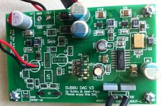
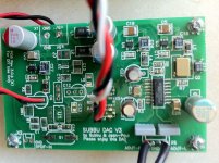
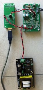
Some pics of my DAC V3 Beta with PSU and Amanero/Isolator.
I'm very very surprised by the result of this combo, sound is very detailed, with a great deep scene and clean soundstage using standard caps... still the same natural bass presence I've really appreciate in previous v2.6. Seems very promising to me, let's have some burn in time for my ears 😉
I've bended and soldered a standard 3x2.54mm pins on I2S PCB traces.
After some troubles, I've reduced I2S cables lenght, works fine.
Some improvments could be expected on this side.
Great to read that there will be different dedicated versions.
Everyone could pick his prefered flavor 😎
I've tested my board with I2S only, SPDIF part unpopulated, except one PSU line required for USB/isolator (3.3v).
Some pics of my DAC V3 Beta with PSU and Amanero/Isolator.
I'm very very surprised by the result of this combo, sound is very detailed, with a great deep scene and clean soundstage using standard caps... still the same natural bass presence I've really appreciate in previous v2.6. Seems very promising to me, let's have some burn in time for my ears 😉
I've bended and soldered a standard 3x2.54mm pins on I2S PCB traces.
After some troubles, I've reduced I2S cables lenght, works fine.
Some improvments could be expected on this side.
Great to read that there will be different dedicated versions.
Everyone could pick his prefered flavor 😎
Attachments
Last edited:
Nice setup 🙂
However I am wondering about the missing GND connection for the I2S lines. High speed signals (take a look at Chris/hochopepers post) always need a low impedance ground return path. In your configuration ground return currents have to take the power supply line route which is not low impedance at all. Thus I'd add at least one GND line to the 3 I2S lines...
However I am wondering about the missing GND connection for the I2S lines. High speed signals (take a look at Chris/hochopepers post) always need a low impedance ground return path. In your configuration ground return currents have to take the power supply line route which is not low impedance at all. Thus I'd add at least one GND line to the 3 I2S lines...
Nice setup 🙂
However I am wondering about the missing GND connection for the I2S lines. High speed signals (take a look at Chris/hochopepers post) always need a low impedance ground return path. In your configuration ground return currents have to take the power supply line route which is not low impedance at all. Thus I'd add at least one GND line to the 3 I2S lines...
Correct ! We removed the I2S possibility from his version so it is solved.
Correct ! We removed the I2S possibility from his version so it is solved.
That sounds good. The separate types will surely be the best way; being specifically designed for what it needs IE: SPDIF or I2s instead of being all things at once.
Will the I2S pcb have g-s-g-s-g-s-g-s terminal ? Or only u.fl ? It will be smaller ?
The group buy document has only one pcb to select. There are >300 people. I think you must make clear the details of the project(s) and change the document, i.e v3.1, v3.2, v3.3 etc or you will have much trouble ;-) But it is for you to choose. 🙂
The group buy document has only one pcb to select. There are >300 people. I think you must make clear the details of the project(s) and change the document, i.e v3.1, v3.2, v3.3 etc or you will have much trouble ;-) But it is for you to choose. 🙂
Keep it cool Nanoloop, informations will be updated when confirmed.
I2S and SPDIF boards and BOM will be added and updated in the Magic Spreadsheet :
https://docs.google.com/spreadsheet/ccc?key=0Akhn9Qkz5rm9dDNBeUNGZE4zbm1oVGpwRUtyd0NadlE#gid=0
By now, the "Wizard Team" (Jean-Paul & Subbu) is still cooking...
Regards
Phil
I2S and SPDIF boards and BOM will be added and updated in the Magic Spreadsheet :
https://docs.google.com/spreadsheet/ccc?key=0Akhn9Qkz5rm9dDNBeUNGZE4zbm1oVGpwRUtyd0NadlE#gid=0
By now, the "Wizard Team" (Jean-Paul & Subbu) is still cooking...
Regards
Phil
Last edited:
I am very relaxed, thank you. 🙂 Curryman is correct. The test is the example of the wrong (?) pcb used in the wrong way, so I do not understand. If you say there is many boards but have only spdif for the bad hack, what can I think ? I'm very sorry for the comments. Should I say nothing ? I think yes, and I find other. So sorry.
Some informations, to be clear 😉
My setup is for testing purposes only, I've decided to go the I2S way.
I've previously told that my I2S section could be improved. (Post#726)
Those boards are "Beta", not final design for the GB.
From what Jean-Paul told few posts ago, there will be 2 PCB versions : I2S and SPDIF.
Thanks to curryman for pointing his tips concerning I2S/Gnd. This will be done with next I2S PCB revision.
Regards
Phil
I am very relaxed, thank you. 🙂 Curryman is correct. The test is the example of the wrong (?) pcb used in the wrong way, so I do not understand. If you say there is many boards but have only spdif for the bad hack, what can I think ? I'm very sorry for the comments. Should I say nothing ? I think yes, and I find other. So sorry.
I think you should start drawing one yourself and leave ours for what is is. We don't have any obligation towards anyone. If you consider I only needed 1 DAC myself and now I am making the nth version you probably understand that it is easier to comment that to design and build.
you dont have any obligation? sorry, I beg to differ. you have strung 300 people along for ~6 months. (estimate, several anyway)
maybe this was just poorly chosen words above, but it comes off as flippant/callous.
I think people do appreciate what you are doing, I for one know how much work a GB is, but you do have an obligation to be clear about what you are offering at this point. people have been patient you have to agree yes? whether this responsibility is what you had in mind or not, a responsibility you have. I can understand why it could get daunting and seem too hard work, but that is the monster you have created 😉
there are several good examples of how to use the u.fl and w.fl connectors on these forums, as well as the datasheet. inductance is the enemy of HF grounding, return paths should be as direct as possible.
Last edited:
qusp, I understand your point, though, in this case I agree with J-P:
Though I think there is another option that J-P is leaving out there; there are already designed ES9023 PCBs that allow i2s input.
J-P has always been clear that his preference was for SPDIF source and it took priority. There has been some consideration of accommodating others where possible. People took the chance to wait based on comments that there would be an attempt to accommodate i2s input, maybe this will eventuate in a future offering from the contributors in this thread.
Some of the examples of good u.fl implementations also have positions for es9023 DAC chip and are already relatively inexpensive. I can think of at least three active forum members who each have each offer examples of bare PCBs for the DIYer that meet the needs of people wanting i2s input to a ES9023 DAC, two of them offer u.fl inputs.
If time is a critical issue for an individual on this GB and they need something sooner they should design themselves, buy one that is available that suits their technical requirements or wait for a future revision that may meet their needs.
This is DIY not join the biggest list and hope that it meets what I need. GB subscribers, I hope, are making informed technical decisions.
My number one priority is that I help other DIYers make informed technical decisions on what their requirements are and decide for themselves which option best meets their need.
I think you should start drawing one yourself and leave ours for what is is.
Though I think there is another option that J-P is leaving out there; there are already designed ES9023 PCBs that allow i2s input.
J-P has always been clear that his preference was for SPDIF source and it took priority. There has been some consideration of accommodating others where possible. People took the chance to wait based on comments that there would be an attempt to accommodate i2s input, maybe this will eventuate in a future offering from the contributors in this thread.
Some of the examples of good u.fl implementations also have positions for es9023 DAC chip and are already relatively inexpensive. I can think of at least three active forum members who each have each offer examples of bare PCBs for the DIYer that meet the needs of people wanting i2s input to a ES9023 DAC, two of them offer u.fl inputs.
If time is a critical issue for an individual on this GB and they need something sooner they should design themselves, buy one that is available that suits their technical requirements or wait for a future revision that may meet their needs.
This is DIY not join the biggest list and hope that it meets what I need. GB subscribers, I hope, are making informed technical decisions.
My number one priority is that I help other DIYers make informed technical decisions on what their requirements are and decide for themselves which option best meets their need.
you dont have any obligation? sorry, I beg to differ. you have strung 300 people along for ~6 months. (estimate, several anyway)
maybe this was just poorly chosen words above, but it comes off as flippant/callous.
I think people do appreciate what you are doing, I for one know how much work a GB is, but you do have an obligation to be clear about what you are offering at this point. people have been patient you have to agree yes? whether this responsibility is what you had in mind or not, a responsibility you have. I can understand why it could get daunting and seem too hard work, but that is the monster you have created 😉
there are several good examples of how to use the u.fl and w.fl connectors on these forums, as well as the datasheet. inductance is the enemy of HF grounding, return paths should be as direct as possible.
1. You are taking my words out of context but still I will react on the obligation thing. Even if it would be a million people it would not change. I have no obligation to change the device to the taste of someone else just as people have no obligation to buy what we create. You are pointing on an obligation that we "have to deliver" according you. Also that is no obligation although we are doing our best to deliver. We are talking about a PCB for a few dollars here i.e. luxury goods albeit with a low value. It is nice to have but does your life depend upon it ? No. Does our life depend upon it ? No. Can I stop today and quit ? Yes. Let me say that I haven't experienced the same sense of quality and commitment in such projects otherwise i would not be doing this.
2. I am not a native english speaker and here we are also quite direct in wording. This can often be misunderstood by native english speakers who often like to express themselves with contra-dictionary comment in our view. So excuse me for the "poorly chosen words". Interesting !
3. You also seem to have misunderstood what I meant. The U.FL have been dropped on the SPDIF version of the PCB as they don't have a function on it. Even if they would be the best choice on whatever PCB , I still think they are the crappiest connector on this planet. Which does not mean that I won't use them as they are kind of a standard.
We try to make a nice device and put time in something that also costs us effort and money. No more no less.
Last edited:
I think you should start drawing one yourself and leave ours for what is is. We don't have any obligation towards anyone. If you consider I only needed 1 DAC myself and now I am making the nth version you probably understand that it is easier to comment that to design and build.
I'm sorry if my meaning is not clear. I think that spdif is the number 1, so for I2S, maybe never, so I ask for some basic ideas like gsgsgs etc.
I know it is not easy. For example, my baby-step for layout idea. Power line under the IC..... oh no... but there can be advantage...
Anyway, I wish you success 🙂 I find the other project.
Attachments
- Status
- Not open for further replies.
- Home
- Group Buys
- ES9023 / WM8804 S/PDIF "Subbu DAC V3" GB Interest