Leach's analysis is just wrong, the forward path has no dependence on the feedback network.
Come now, Scott, you KNOW, surely, that forward path gain in a so-called "CFA" is affected by the the Thevenin impedance of the feedback network as "seen" from the inverting port because this impedance constitutes the emitter impedance of the common emitter input stage.🙄
Ok, say 60dB @ 20KHz or 50dB @ 60KHz...
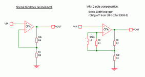
Think double pole compensation: the loop gain is still rolling off at a two pole rate at 20KHz.
Good thinking. Of course you can use 2-pole compensation with a so-called CFA as well. No particular reason you can't have 60dB loop gain at 20KHz with a "CFA" either. What was your point again?Think double pole compensation...
Good thinking. Of course you can use 2-pole compensation with a so-called CFA as well. No particular reason you can't have 60dB loop gain at 20KHz with a "CFA" either.
You really can't have double pole compensation with the traditional single gain stage "CFA" with current mirrors as the minor loop requires an inverting gain stage to work. That's my point.
Yes you can, even with the CFA opamp chips. Here's an example of how to do it:You really can't have double pole compensation...
edit: That example assumes the input impedance of the inverting input is zero. If it's 50 Ohms, set R2 = 470R, R3 = 47R.
Attachments
Last edited:
Interesting; would have to run a sim to see whether it really works.
Is the amplifier internally shunt compensated as well?
Is the amplifier internally shunt compensated as well?
Yes, same shunt cap in each case.
As an aside, you can achieve the same effect with a typical VFA by connecting an inductor between the emitters of the LTP (assuming it was resistively degenerated to start with).
In another thread, someone mentioned a discreet opamp with inductors (presumably with parallel resistors) in series with the emitters of the LTP. A side benefit may be better immunity to RFI at the input, but then again the coils might pick up RFI themselves. :/
Last edited:
Because minor loop compensation of the shunt derived shunt applied variety can only be implemented around an inverting gain block (transimpedance stage). Nothing of the kind is to be found in the usual so-called "CFA".
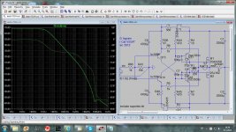
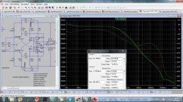
How you then explain difference in Loop Gain between those two simulations, one with MC other with TMC? Distortion at 20kHz is down by 14dB compared with MC.
Look also here.http://www.diyaudio.com/forums/solid-state/233056-what-about-amp-cfa-vfa-2.html#post3434413
BR Damir
Attachments
How you then explain difference in Loop Gain between those two simulations, one with MC other with TMC? Distortion at 20kHz is down by 14dB compared with MC.
Look also here.http://www.diyaudio.com/forums/solid-state/233056-what-about-amp-cfa-vfa-2.html#post3434413
BR Damir
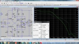
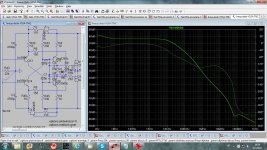
Before explaining anything (and talk about a 10MHz ULGF), put some resistors in the MOSFET gates.
All i can see is a single pole roll off in both cases.
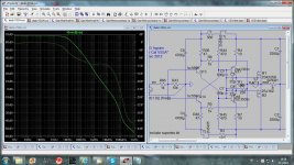
OK here the amp is a bit change and it's possible to see that there are two poles, and Loop Gain bandwidth is extended from 2kHz to 11kHz (-3dB).
By the way this was quick TMC component selection, it could be better optimized
Attachments
Last edited:
Before explaining anything (and talk about a 10MHz ULGF), put some resistors in the MOSFET gates.
This is just simulation and adding the gate resistors does not change much.
Attachments
Level shifting in the case of the complimentary common emitter "CFA" is transfering the AC changes in the input stage's collector current to the load without altering them in any way. This is the purpose of the current mirrors. Now, why can't a phd candidate see this?
If you cant see that a so-called "CFA" has a voltage divider draped across its output that delivers a fraction of the output voltage to the inverting input of your so-called "CFA", then you're really beyond help.
At least Professor Leach and Professor Cherry were able to see this most elementary of facts.
Not so. The voltage divider draped across the output feeds a low Z EF output w/ a few ohms of resistance. The Thevenin Z at this node is dominated by the very low Z of the EF output, a few ohms. The voltage at this node, Vn, is determined by the EF, so that it forces Vin to appear at Vn. To illustrate one only needs to break the servo loop by removing Rfb. The output will go to the rail, byt Vin will remain at the value of Vp=Vin. The EF forces Vn to follow Vp, of course "emitter followers" are so named. The Vp node being driven to match Vp is done by the input EF, not the servo loop.
Use a simulator, or the lab bench, and you can see for yourself. The fb resistive "divider" in a CFA functions differently than a VFA. The process of "divider action" you envision, holds true only in the VFA. The Vn value is simply a divided down value of Vout. If the servo loop is opened by removing Rfb, the - input floats, there is no means by which to force Vn to follow Vp.
Breaking the servo loop in a CFA results in the - input Vn remaining as is, it follows Vp being forced to do so by input EF stage. This can be proven in a few minutes. If you don't wish to simulate or use the bench, just examine my schematic. It's all there. The reason "I can't see the voltage divider" is because it isn't there.
We discussed Cherry 8 yrs, ago and we arrived at a near unanimous view that Cherry stated "if the input buffer is removed and replaced with a differential pair, and the current mirrors replaced with a CE stage, then a CFA is realized"!!! Of course, no argument there. The error signal is In, the current entering/exiting the - input. I illustrated 8 yrs. ago. Good day.
Claude
Because of the x20 feedback resistor (R5/R6) over the emitter resistors (R36/R40), this is barely a real "CFA", but more like "a CFA topology in VFA mode" as described above. 1kohm barely loads the input node and therefore modifies the forward gain (through the transconductance of the input stage).
What am I missing, there is a 1K || 47 Ohm divider. 47 ohm equivalent resistance to ground.
Input stage still provides equal base voltage splitting versus a vfa which results in equal current splitting.
Thanks
-Antonio
What am I missing, there is a 1K || 47 Ohm divider. 47 ohm equivalent resistance to ground.
Input stage still provides equal base voltage splitting versus a vfa which results in equal current splitting.
I'm not looking from this perspective. You have a circuit/black box with a output parallel and input series feedback. According to the canonical approach, you characterize this with forward and reverse hij parameters. To calculate the forward gain h21, you need to break the feedback loop and consider the loading of the feedback network on the forward gain.
Accordingly, and considering only half of the circuit, the output is loaded by R6+R36 (and can be ignored) while the input is loaded by R6 || R36. R6 >> R36 (1kohm vs. 47ohm) which means this loading can be largely ignored as well.
This is exactly the situation of a VFA. If you apply the same canonical method to a standard VFA (with long tail pair, etc...) you get to the same conclusion: the feedback network loading can largely be ignored.
Now consider what's happening when R6 would be comparable to R36. Then the loading R6 || R36 can no longer be ignored. I have already mathematically proved that in the particular case of the CFA topology under discussion, this loading modifies both the forward gain and the crossover frequency, hence the CFA properties of constant bandwidth (and also the known property of "feedback resistor provides frequency compensation").
Therefore, the CFA properties are occurring only for smaller values of R6 (mapping to lower closed loop gains). For the values in the schematic, the amplifier behaves largely as a VFA.
Please observe that I made no use of any empirical (and otherwise correct) observations like "low impedance node", "current summing" and assumptions about where the current is flowing, etc... but only the good old control theory. The main result is that ultimately a CFA is a particular case of a VFA (in the control theory sense, so an amplifier which is canonically modeled by it's forward and reverse hij parameters), where the forward gain and crossover frequency are modulated by the feedback network.
Not so. The voltage divider draped across the output feeds a low Z EF output w/ a few ohms of resistance. The Thevenin Z at this node is dominated by the very low Z of the EF output, a few ohms.
Your appreciation of the most basic circuit theory is truly lamentable.🙁
As far as the inverting port is concerned, the " very low Z of the EF output" appears as a virtual ground so that the two feedback resistors appear in parallel. Elementary my dear Watson! 🙄
The fb resistive "divider" in a CFA functions differently than a VFA. The process of "divider action" you envision, holds true only in the VFA.
No.😀
We discussed Cherry 8 yrs, ago and we arrived at a near unanimous view that Cherry stated "if the input buffer is removed and replaced with a differential pair, and the current mirrors replaced with a CE stage, then a CFA is realized"!!! Of course, no argument there. The error signal is In, the current entering/exiting the - input. I illustrated 8 yrs. ago. Good day.
Claude
You obviously didn't read Cherry's paper or you didn't understand the little that you read otherwise you wouldn't take it out of context so grotesquely.😀
And when you speak of "a near unanimous view" you should really speak for your self only.

Last edited:
We discussed Cherry 8 yrs, ago...
Claude, here is what Cherry said about the so-called "CFA":
So get your facts straight Claude!😎The feedback connection is voltage sensing at the output and voltage subtracting at the input; the circuit is an ordinary voltage gain feedback amplifier. The term "current feedback amplifier" seems a complete misnomer.
Last edited:
Your appreciation of the most basic circuit theory is truly lamentable.🙁
As far as the inverting port is concerned, the " very low Z of the EF output" appears as a virtual ground so that the two feedback resistors appear in parallel. Elementary my dear Watson! 🙄
No.😀
You obviously didn't read Cherry's paper or you didn't understand the little that you read otherwise you wouldn't take it out of context so grotesquely.😀
And when you speak of "a near unanimous view" you should really speak for your self only.
Cannot be. If the EF output was "virtual ground your argument collapses on its own. The other end of the resistor from - input is also grounded, hence this resistor is shorted out making the equvalent Z near zero. It cannot be R1 || R2, because the R1 would have 1 terminal at ground and the other at your so-called "virtual ground."
Also, if the terminal in question is at virtual ground, how can it have "Vfb". You claim the divider develops a divided down output voltage as the feedback quantity then tell us its "virtual ground". You invent one story after another and they contradict each other.
I read the whole Dr. Cherry paper and I quoted him correctly, rerean 8 yrs. ago my post and the follow ups. Every OEM describes error signal as "In", if Dr. Cherry differs (I don't know that he does), he has given no proof that error signal is a voltage. You seem to think he agrees with you, perhaps he does, but his believing so is not proof.
Every network, device, amp, etc., that is described as "current mode, feedback, controlled, etc." always generates controversy. There is never a hostile debate about VFA devices or anything coined as "voltage-mode". Some, a minority, do not accept anything as defined w/ current as the control or error signal, only voltage. So all current mode device discussions bring about debates, but not with voltage mode.
Anybody can find someone, Dr. Cherry, or whoever, that disagrees with "current-mode" classification. Some people will never accept any device classified as current mode, period. You are such a person. I'm not belittling your ability, I'nm just saying that you are much more comfortable w/ voltage as the control signal, and current as incidental.
Claude
...
Now consider what's happening when R6 would be comparable to R36. Then the loading R6 || R36 can no longer be ignored. I have already mathematically proved that in the particular case of the CFA topology under discussion, this loading modifies both the forward gain and the crossover frequency, hence the CFA properties of constant bandwidth (and also the known property of "feedback resistor provides frequency compensation").
Therefore, the CFA properties are occurring only for smaller values of R6 (mapping to lower closed loop gains). For the values in the schematic, the amplifier behaves largely as a VFA.
...
Waly,
Thanks for trying I guess I just dont agree.
How does loading of the input stage only occur as the Rf is near Rg or gains near 2. The input stage doesn't know which resistor is loading it, indeed the open loop gain is directly proportional to the inverse of the equivalent resistance seen by the emitters (emitter "error" current x HiZ node), the closed loop gain is simply the result of the resistor ratios.
Thanks
-Antonio
- Status
- Not open for further replies.
- Home
- Amplifiers
- Solid State
- Current feedback - Voltage feedback, how do I see the difference?