Hi
I found a class A circuit from Mullard transistor audio and radio circuit.
Hi thanks.
Am I the only one? AFAIR I have never found anything good associated with Mullard 😀
Mullard Pi mode class A
This circuit has been discussed in this thread:
http://www.diyaudio.com/forums/solid-state/100736-mullard-ss-power-amplifier.html
--gannaji
--------------------------------
www.Samritatrust.org
Hi
I found a class A circuit from Mullard transistor audio and radio circuit. I thought it may be useful to someone in this thread. Please see the attached pdf file for text and circuit.
This circuit has been discussed in this thread:
http://www.diyaudio.com/forums/solid-state/100736-mullard-ss-power-amplifier.html
--gannaji
--------------------------------
www.Samritatrust.org
Last edited:
Hi Mike,
Interesting circuit you have there (I think I have never seen it before 😕). You're right, I will also be interested to see an all-FET version of your circuit. But I have different plan for my mosfets 😀
I think I will build your amp. What is that resistance in series with power supply cap? How much current running through each output transistor and driver? What is the possible range of the rail voltage? Why is the 1pF at the input?
Glad ur interested Jay
That Resistor just repesents PSU internal impedance.
1pF just left there by mistake
Suggest you build it in spice first to get your head around it.
I would make voltage about 22 - 24V
The current was it's weak point it, was too low, can't remember exactly what now perhaps 1.3A. I would suggest 2 - 2.5A per side
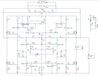
Your interest has inpired me and aroused a feeling of responsibility to offer you a half decent up to date diagram.
So I just revamped it to what I would to now - will post shortly
Here it is.
Had to go to mosfets - just works better with them
I used irfp044n's - Lateral would be better but didn't have models for them in this spice program.
The three red resistors are trimmers & are used for set up
Top one adjusts o/p voltage - set to midpoint
Bottom two adjust o/p stage bias current.
This simulates much better that previous posted circuit particularly HD & Stability.
cheers
mike
p.s. i/p 100pF should be removed if u use 10R series i/p resistors
Attachments
Last edited:
One more question: how about moving the CRC to the front of the shunt regulator?
Forget this one 😀
Your interest has inpired me and aroused a feeling of responsibility to offer you a half decent up to date diagram. So I just revamped it to what I would to now - will post shortly
Thanks Mike.
I wont probably build the mosfet version soon enough because I have many others already in the waiting list (on going).
But the bipolar version is a must build for me because of many reasons:
(1) I have plenty of heatsinks
(2) I have hundreds of NPN-only bipolars, mostly in TO-3 (4-16MHz)
(3) The only topology I trust for "quasi-complementary" bipolar amp is the JLH
(4) I want single ended supply because I like a limited number of big caps in the power supply, and I have many single-secondary transformers. And the charm here is the in-existence of output cap!
(5) I think the balanced circuit will improve efficiency?
(6) etc
So it is very likely that I will keep this amp, and wait for future upgrades 😉
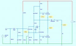
I decided to play around around with the original design to see if I could arrive at a good upgraded version. Still thinking in terms of a balanced final product but using the simple S/E version to avoid doing everything twice.
I tried different approaches in every part of the cct and this is where I ended up. I would regard this as a good starting point and try some variations in real life.
As well as focusing on HD & stability I tried to find a topology that got the best current sharing between the o/p devices. The boot strap beat everything else in this regard giving a possible 3A peak at the O/P with a 2A standing current. This in conjuction with i/p cct CCS & MF driver also gives very good HD figure.
Attachments
Mike?
2200000uF?!?!?!?!
😱
Also is that resistor (4Ohm) the output load? Do you not simulate with a complex impedance? Maybe im missing something here
2200000uF?!?!?!?!
😱
Also is that resistor (4Ohm) the output load? Do you not simulate with a complex impedance? Maybe im missing something here
hehe,
If I make a balanced version ( which JLH referred to in one of his early articles ) then the caps can be removed . . . . . so I made it big enough to become virtually invisible.
I don't have a 2.2F cap in my Box !
🙂
If I make a balanced version ( which JLH referred to in one of his early articles ) then the caps can be removed . . . . . so I made it big enough to become virtually invisible.
I don't have a 2.2F cap in my Box !
🙂
post2330,
why a mosFET as the input device?
Would a jFET do the job?
Would a jFET reduce the performance in any way?
why a mosFET as the input device?
Would a jFET do the job?
Would a jFET reduce the performance in any way?
post2330,
why a mosFET as the input device?
Would a jFET do the job?
Would a jFET reduce the performance in any way?
I would suggest a socket to allow quick subjective assessment of different i/p devices.
In spice the mostfet gave a slight gain / phase advantage over a BJT so I left the mosfet in place.
Didn't simulate with a jfet but worth a try. OLG might be less with Jfet
The i/p cap could be 1uF ( 100uF was just an experiment )
mike
Last edited:
Hi Mike!
As far as I can see: The load at top and bottom of the phase splitter is not the same ACwise ( 154 ohm and 77 ohm ). Meaning that you are feeding the upper output device twice the voltage as the bottom device. This would not be a problem with BJT outputs, as they are current controlled, and AC current would be the same on top and bottom of the phase splitter. Not so with MosFets.
Thorsten Larsen
Hi thorsten,
The driver stage resistance values are just governed by ohms law - no choice in the ratios for a given current otherwise the o/p will not be centred between the rails.
These are not complementary o/p devices comparing those two values is not really valid. The o/p devices are not that sensitive to driving impedance so this is not such a big deal - check it out in spice I think you will see that it works quite elegantly.
Actually under detailed spice analysis of current sharing, this o/p arrangement performed better than anything else I tried - so much more elegant than using a CCS in the driver stage.
Hope this clarifies to some extent.
edit: perhaps the boot strap resistor values could be experimented with - didn't try that - but I wouldn't expect the difference to be enormous.
Last edited:
Can anyone advise the best voltage to use with 8ohm speakers? These boards are for a single rail supply only and not split rail?
What are the variable resistors for? Dc offset?
Is there a specified adjustment proceedure on start-up?
What are the variable resistors for? Dc offset?
Is there a specified adjustment proceedure on start-up?
I'm afraid that you read a little bit more on how to build this thing and how to fire it up, else you'll probably fire it up.Can anyone advise the best voltage to use with 8ohm speakers? These boards are for a single rail supply only and not split rail?
What are the variable resistors for? Dc offset?
Is there a specified adjustment proceedure on start-up?
In short, be sure to have low rail voltage (eg 5V or so) and have one of these variable resistors adjusted so that you have minimum bias current. Then adjust DC offset, let it warm up a little more and keep DC offset small.
The start increasing bias current. If everything is still ok, go for higher rails voltage and gradually work your way up to the desired Ig (bias current) while keeping DC-offset close to 0.
succes, MArco
P.S. don't forget to read more ...
siliconray boards are dual(split) rail.
VR1 and VR2 is DC-ofsett adjust.
VR3 is bias.
+/-23-24V.
so 2x18V transformer.
VR1 and VR2 is DC-ofsett adjust.
VR3 is bias.
+/-23-24V.
so 2x18V transformer.
Last edited:
siliconray boards are dual(split) rail.
VR1 and VR2 is DC-ofsett adjust.
VR3 is bias.
+/-23-24V.
so 2x18V transformer.
Brilliant. Thanks.
Should I aim for 5v Bias current?
- Home
- Amplifiers
- Solid State
- JLH 10 Watt class A amplifier