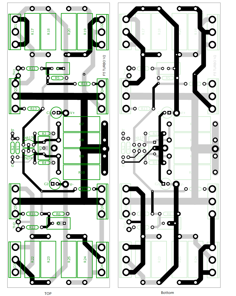
Learn to draw an V2 PCB for myself, any comments are welcome! 😱
PS: right click for the image url to get larger resolutions image
R3 & R4 should be bigger as they pass the feedback current.
Input ground an decoulping one should be separated and then only join a common point.
Input circuit is surrounded by output devices. I would prefer to keep it a bit apart.
On a fast glance.
Input ground an decoulping one should be separated and then only join a common point.
Input circuit is surrounded by output devices. I would prefer to keep it a bit apart.
On a fast glance.
Last edited:
Learn to draw an V2 PCB for myself, any comments are welcome!
I'm rather new around here so my apologies in advance for a possibly daft question.
Which software did you use for this PCB design? Everybody else, please chip in - is there such a thing as strongly preferred/standard package? Free?
Thanks, Mike
I'm rather new around here so my apologies in advance for a possibly daft question.
Which software did you use for this PCB design? Everybody else, please chip in - is there such a thing as strongly preferred/standard package? Free?
Thanks, Mike
There is a free download called Design spark it has all the funtionality of
Easypc which I have bought for £350 and even beter components library
It was made in collaboration with RS components.
It was recentley advertised in Elektor magazine.
Being Free you may give it a go certanly you got notthing to loose.
Just gogle up Design spark.
Altrough not needed if you cook your own board it has output for gerber and such
That is the only standard one need for professional output/ functionality.
Pin spacing and track size and so on is al there
Last edited:
Prelimenary Layout for F5 v2
Comments and critisicsm always welcome.
Best Regards
Andy
Comments and critisicsm always welcome.
An externally hosted image should be here but it was not working when we last tested it.
An externally hosted image should be here but it was not working when we last tested it.
An externally hosted image should be here but it was not working when we last tested it.
Best Regards
Andy
Forgot to say;
Board is 350mm x 50mm.
Phoenix connectors for Input, Output and Power.
Minimum track width 1.2mm (1.6mm on output devices).
1.6mm board woth 2oz copper.
Board is 350mm x 50mm.
Phoenix connectors for Input, Output and Power.
Minimum track width 1.2mm (1.6mm on output devices).
1.6mm board woth 2oz copper.
Massimo.
Can you translate mils to mm please.
I wasn't planning on etching at home. I'll get some made with proper solder resist and silkscreen.
Andy
Can you translate mils to mm please.
I wasn't planning on etching at home. I'll get some made with proper solder resist and silkscreen.
Andy
Massimo.
Can you translate mils to mm please.
I thought UK was imperial, while the rest of Europe metric.... 😉
1 mil = one thousandh of inch = 0.0254 mm
Toecutter:
My main criticism with your layout is that the high current paths must be MUCH larger. These are all of the paths from the V+/V- supply rails thru the source resistors, diodes, output mosfets, and to the output terminals. Similarly, the connection ffrom the power supply ground to the speaker ground must be larger. There could be star-grounding issues related to R3, R4, and P3. Best that that ground be derived more directly from the ground at the input connector block.
There are also (less serious) signal currents thru the feedback resistors R7-R10 that suggest larger traces. In general, there is little or no cost associated with using large traces. For the highest current paths, you can also run traces on both sides of the board, connected with additional vias.
Yes, looks like star grounding issues.
Input jfets benefit to be in touch for temperature tracking.
Input jfets benefit to be in touch for temperature tracking.
Last edited:
350MM probably makes it too big to fit into the common Conrad heatsinks a lot people use. A little smaller might be nice, only if this is something you plan on getting rid of.
What size are the conrad heatsinks?
Maybe this help single sided duble mosfets cascoded duble imputs.
No current limiters space for 2 futabas source resistors
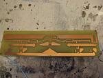
Sorry crapy picture was on MYF5 tread may see better there
At work at present but can do better tomorow if you like
No current limiters space for 2 futabas source resistors
Sorry crapy picture was on MYF5 tread may see better there
At work at present but can do better tomorow if you like
Attachments
Last edited:
Also from same tread
Triple not cascoded the first ones I built.
main thing is no need for duble side and Keep tracks shorth (this is a very fast amplifier and smal parasitic capacitance is a potential problem)
Gate resitor track as shorth as possible to the mosfet pin is realy good advice
Triple not cascoded the first ones I built.
main thing is no need for duble side and Keep tracks shorth (this is a very fast amplifier and smal parasitic capacitance is a potential problem)
Gate resitor track as shorth as possible to the mosfet pin is realy good advice
Attachments

😀Yeah make as one 😀
DesignSpark | The gateway to online resources and design support for engineers
You can get free PCB software from above link
To stick ground plane on anythink it just takes a couple of mouse clicks the real skill which I dont have is to line up the mask to both sides of the board and facing the right way up which I find mind bogling complicated you get more chances to get decent conversation out of potato trough which a direct current is passed than me doing this right the first time
PS all this is in good umor
yeah double sided at home is tough 😀😀😀
I use Sprint ever sine Manu pointed me that way...just what audio guys need ...no more no less 🙂
..and not expensive to boot.
I use Sprint ever sine Manu pointed me that way...just what audio guys need ...no more no less 🙂
..and not expensive to boot.

- Status
- Not open for further replies.
- Home
- Amplifiers
- Pass Labs
- F5 Turbo Circuit Boards