is this schema create by "circuitmaker 2000"?My New thing under creation is Full floating Grounded Bridge 2 step Class-G with ALL N-FETS 😉
if yes, please open the button "OPTIONS" and then "Schematic" and then disable the field "Show Pin Dots" about "General"
Then the circuit is better to read and to understand like my H-bridge circuit in the pdf attachement (based on the "virtual complement" concept, introduced by Bengt Olsson, Electronics World, Dec 1994)
Attachments
Last edited:
Then the circuit is better to read and to understand like my H-bridge circuit in the pdf attachement (based on the "virtual complement" concept, introduced by Bengt Olsson, Electronics World, Dec 1994)
Your circuit has 2 main flaws.
1. No common mode error control, your bridge needs balancing like a bridge centering servo.
2. The Bengt olsson stage you are using suffers from huge cross-conduction at high frequecies above 1khz, because the upper mosfet doesn't turns off properly while the lower mosfet is in conduction.
Kanwar
Last edited:
Thank you for redraw and this advices. First advice I understand clearly, but for a simulation task this isn't necessary. Please note: the GND (earth) symbol is arbitrarily set (for getting simulation results) and have not to do with the actually GND line.Your circuit has 2 main flaws.
1. No common mode error control, your bridge needs balancing like a bridge centering servo.
2. The Bengt olsson stage you are using suffers from huge cross-conduction at high frequecies above 1khz, because the upper mosfet doesn't turns off properly while the lower mosfet is in conduction.
Kanwar
Also second advice I also understand, therefore it is to get proper sound only by class-A (hard running) mode.
The same I observe by the last topology from the pdf URL
http://www.ant-audio.co.uk/Theory/N-channel D-MOSFET output stage with improved linearity.pdf
My Opinion was until now, such MOSFETs in general loves idle currents above at least 300mA.
Mr. Bob Cordell and an other member tell me by post #14 about
http://www.diyaudio.com/forums/soli...s-ab-overview-p-spice-urls-2.html#post2569135
that is no true - 7mA are enough for good results, as to observe by several power amps from the brand "Peavey" (without mention of model No examples). If I have time, I will investigate this.
Last edited:
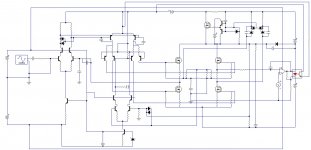
NVMOS AMPLIFIER
Send a message via Yahoo to Workhorse
Hi Rahul,
Have a look at this latest schematic for your easy to see reference....
Any further progress made so far by you?
regards,
K a n w a r
Attached Thumbnails
NVMOS amplifier-ampdiy.jpg
Hi Workhorse
greetings is schematic on post 252 final and is it ok for build
warm regards
andrew lebon
NVMOS AMPLIFIER
Hi Workhorse
greetings is schematic on post 252 final for me to try out this amp
have designed a simple pcb how many watts should i get with 6 pairs IRF460
using 80 volts dc rails have many 460 so i try your wonderful amp
warm regards
andrew lebon
Hi Workhorse
greetings is schematic on post 252 final for me to try out this amp
have designed a simple pcb how many watts should i get with 6 pairs IRF460
using 80 volts dc rails have many 460 so i try your wonderful amp
warm regards
andrew lebon
NVMOS AMPLIFIER
Hello Workhorse Sir
greetings i am a new member of diy audio i would like to make this
amplifier little confused which schematic to refer to i can make a simple pcb for it only
need little guidance please can you help me as this is my first project in electronics ONLY please tell me wich circuit post to follow
warm regards
sameer x1
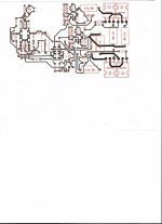
..... PCB for post # 252 layout in few hours 🙂
Regards Alex.
Regards Alex.
Attachments
Last edited:
maestro at work
Hi Alex mm
greetings nowadays even i am trying sprint just love your
work really proffessional
warm regards
andrew lebon
Hi Alex mm
greetings nowadays even i am trying sprint just love your
work really proffessional
warm regards
andrew lebon
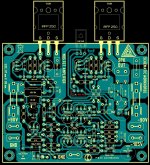
..... thank you @andrewlebon , but small transistors are for 2SA970 and 2SC2240 , sorry for this error , I noticed just now ....🙁
Alex.
Alex.
schematic you are following
Hi Alex mm
greetings can you please refer to which schematic you are following
for pcb you posted waiting for you to complete pcb to try out how amp performs
warm regards there is also a positive15 volt supply
andrew lebon
Hi Alex mm
greetings can you please refer to which schematic you are following
for pcb you posted waiting for you to complete pcb to try out how amp performs
warm regards there is also a positive15 volt supply
andrew lebon
..... PCB for post # 252 layout in few hours 🙂
Regards Alex.
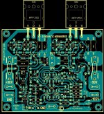
Nice attempt,
The MJE340 must be mounted to heatsink close to mosfets, it controls the bias and needs thermal feedback from heatsink. Either change the layout or you need to mount the device through wires. Also the holes of Zener 15V 1W looks small. Pinouts of MPSA transistors are also wrong.
Last edited:
Quick Job
HI Alex,
I am amazed how quick you did the layout after talking to you about doing a board for the NVMOS amp.
Do the suggestions made by Workhorse who is the designer of the amp and it will be a slam dunk.
You made it more plain when you used -105 volts instead of -15vdc referenced to the -90vdc supply. Good idea,less confusing.
This board layout is from post #252.
Listen to what Workhorse says and you will come out with a great pc board.
Thanks for taking on this project.
Sam
PCB rev 2
.... I have done something , this evening, so I can show you the layout 🙂
Thanks for comments .
Regards Alex,
.... I have done something , this evening, so I can show you the layout 🙂
Thanks for comments .
Regards Alex,
Attachments
Last edited:
Looks much better now🙂 , how about increasing the pad size of components, owing to the fact that its a single sided non PTH PCB.
mosfet choice
Hi Workhorse
greetings which is the most suitable mosfet for this amp
IRF 250 IRF260 IRF460 for best results nice to see this thread moving
warm regards
andrew lebon
Hi Workhorse
greetings which is the most suitable mosfet for this amp
IRF 250 IRF260 IRF460 for best results nice to see this thread moving
warm regards
andrew lebon
pcb
Dear Sir Alex mm
hello will you share pcb for diy can it be used in 4 ohms
thanking you
dilip
Dear Sir Alex mm
hello will you share pcb for diy can it be used in 4 ohms
thanking you
dilip
- Status
- Not open for further replies.
- Home
- Amplifiers
- Solid State
- NVMOS amplifier