Hi VHF,
have you built a CFB VAS into TMCed amplifier?
Is it easy to stabilise. Any other issues we need to be aware of?
Is the CFP equivalent to the EFed VAS in terms of the extra VAS gain required to allow TMC to work effectively?
Good questions.
I haven't as yet used TMC with the CFP VAS but I have built and compared blameless amps with CFP and darlington VAS and CFP was a clear all round winner. The only issue I ever encountered was a tendancy to oscillate at HF - VHF frequencies when employed using high ft devices (as CFP's tend to do) but the cure is a simple ferrite bead at the VAS emitter. The SQ is obviously better without the parasitics but I also found that F14 was the best ferrite for SQ, although I haven't investigated this further.
FWIW my prototype amp produced < 0.0002% THD. My PC based analyser was not able to show marked differnces between VAS types but the CFP VAS did produce slightly less odd order. Perhaps that's why it scored better in SQ tests (?).
The CFP can be easily 'tuned' to produce the same beta as a darlington VAS so I would expect the amount of TMC distortion reduction to be every bit as good. I don't have a good LT library of transistor models - so if someone wants to sim the CFP with optimum devices I would also be interested to see the results for confirmation. I am currently building the alt2 PCB but it might be a week or two before completion.
cheers, vhf
Last edited:
David
I suspect that your results, both subjectively and objectively, are improved further because you are only using EF output doubles, not triples ?
I believe that one of the major reasons this project stalled was the insistence by some members on the use of triple output devices, which made the use of readily obtainable ( cheaper) heatsinks impossible,and suitable metalwork just too expensive to follow through with.
Altronics (Australia) did advertise a suitable "Energy Case" for use with a 2 EF device amplifier, but it never eventuated. That was a shame, as it used the large heatsinks for the sides of the case.
Perhaps Altronic's "cage" needs rattling again by potential Aussie buyers of such a case? Shipping costs to Downunder are prohibitive due to weight, of other suitable cases and metalwork.
Alex
output triples means ?you are only using EF output doubles, not triples ?
or do you mean 2pair vs 3pair output stage?
The usual definition of an EF output double is EF Driver and EF Power Output.
The EF Triple normally is understood to be EF Pre-driver, EF Driver and EF Power Output
output triples means ?
or do you mean 2pair vs 3pair output stage?
The usual definition of an EF output double is EF Driver and EF Power Output.
The EF Triple normally is understood to be EF Pre-driver, EF Driver and EF Power Output
I mean 2 pair vs. 3 pair output stage, which I thought most people would have understood from my references to the need for much larger heatsinks.😉
that was the clue to tell me I was probably misreading what you were discussing.most people would have understood from my references to the need for much larger heatsinks.😉
However, replacing 2pair with 3pair is being done to improve performance into a fixed nominal load impedance.
The extra heat dissipating capability is not being used to deliver more maximum power nor to drive a lower impedance load.
As such the 3pair output devices can be squeezed much closer together than when expecting them to deliver more power where heatsink dissipation becomes critical.
Last edited:
FWIW, the amp sounds fantastic. Much better than any commercial class AB amp I have ever heard and miles ahead of a Meridian 557 that I use as a reference. -vhman
I had the opportunity to listen to David's modified version of this amplifier over approximately a 4 hour period today, and yes, it is VERY, VERY good !😀
SandyK
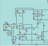
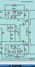
I modified the Ostripper schematic.
The first schematic is what I'm using now and the second (alt2) is the next (preferred) variation.
I am happy. I have just come out with another "preferred" version (below 1/2). I notice the "magic diode". I tried that and no "magic" happened. Since it is sooooo perfect now , we must make it foolproof . R10 , 20 , and 9 plus the 2 separate CCS's seem to do the best ... PSRR wise. Not that it matters a lot , but not tying them together created a very small "thump" for me as the VAS CCS stabilized before the IPS one. 🙁 BTW , I am using a Darlington 2'nd order capacitance mult. to power these front ends now. The schema below has been clipped and abused between 40-75V rails. Also , B. Cordells active VAS current shunt (Q9) seems to both moderate the "unhealthy" clipping characteristics AND any catastrophic current mode. 🙂
I have experimented with R8 in the schema , it shows a decrease of H3 brought to 10K from 2.2K .... but at -130db (below 3 - .00005%) , who would know ?? In conclusion , I think this amp is "killer" , still my main listening amp. 😀
OS
Attachments
I had the opportunity to listen to David's modified version of this amplifier over approximately a 4 hour period today, and yes, it is VERY, VERY good !😀
sandyK... you just couldn't wait to get home and report in, could you. 😀
Yes I have to agree, Dave (VHF man)'s modded SiliconChip ULD MK II is a very nice sounding amp. Well done Dave. I should remind everyone that this amp is built on the original SiliconChip PCBs, not the Ultra PCBs shown earlier in the thread.
Half way through the demo I realised we were listening to a SiliconChip DAC, connected to a SiliconChip preamp (a modded power amp design), connected to a SiliconChip power amp. I am sure sandyK's and Dave's mods have elevated them an order of magnitude, but very impressive results from humble beginnings.
regards
Indeed a good advertisement for SC / DIY kit amps here in Aus. It was also interesting to compare the LM4562HA preamp to Alex's discrete class A pre. The 4562HA was not totally outclassed but the difference was not insignificant.
It's a pity that the new amp will now go to it's new owner but I've already started populating the new boards for the next-G version.
Cheers,
Dave
David
Don't forget those photos before you hand it over.😉
An interesting aspect of David's amplifier, was to me, the internal and external construction. Using the Altronics 20W Class A style metalwork meant that the front panel had surplus holes and printing for the preamp that was not used, and would have let the side down anyway at this level of reproduction.
David overcame this by fitting a quite tasteful wooden front panel.
In subdued lighting, it could just as well been an anodised front panel with a wooden type finish. The amount of heatsinking used was more in line of the requirements of the Class A design, so it never got more than luke warm.
I am happy. I notice the "magic diode". I tried that and no "magic" happened. . 😀
OS
Nice work Os.
FWIW the 'magic' diode concept is intended to enable the current mirror collector voltages to be equalised. I'm not sure if all the benefits can be seen - or are taken into accout in simulations - such as thermal matching, and of course there are nil benefits unless the voltage drops on the loaded side are made equal to those on the regulator side. I actually fine tuned the vas emitter resistor while watching a DmVM across the mirror collectors (via 220k resistors). I can tell you that there appears to be an audible improvement. So the magic diode may not be the best approach in all cases. It really depends on your actual VAS design. For my design it was a + result.
Q9 is a good idea. I saw that implemented in a 1978 design, so it's an oldie but a goodie. 🙂
Cheers
David - vhf man
ref post428
The VAS is biased to ~ 6mA.
0.9mA through Q7 and 5.1mA through Q8.
Q9 will start to turn on when Vbe~400mV.
This requires a current through R17 of ~8mA.
That protection transistor starts to affect audio signal when VAS current rises from 6mA to 8.9mA. R16 current hardly changes with throughput of signal.
That is set far too low.
Full VAS current range is ~8mA+-8mA, i.e. 0mA minimum to 16mA maximum.
I consider that the protection transistor should be set to be just starting to turn on when VAS current reaches it's maximum of 16mA.
I would split the 47r emitter resistor and use the upper half of it as the current monitor for the protection transistor. retain the 47r total value if that is the value that gives best audio performance. 25r+22r would be an acceptable split. 16mA through the 25r portion brings Q9 Vbe to 400mV.
ref post428
The VAS is biased to ~ 6mA.
0.9mA through Q7 and 5.1mA through Q8.
Q9 will start to turn on when Vbe~400mV.
This requires a current through R17 of ~8mA.
That protection transistor starts to affect audio signal when VAS current rises from 6mA to 8.9mA. R16 current hardly changes with throughput of signal.
That is set far too low.
Full VAS current range is ~8mA+-8mA, i.e. 0mA minimum to 16mA maximum.
I consider that the protection transistor should be set to be just starting to turn on when VAS current reaches it's maximum of 16mA.
I would split the 47r emitter resistor and use the upper half of it as the current monitor for the protection transistor. retain the 47r total value if that is the value that gives best audio performance. 25r+22r would be an acceptable split. 16mA through the 25r portion brings Q9 Vbe to 400mV.
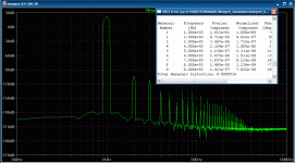
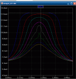
Cordell predicts 27mA with a 22R , I figured 13.5mA with the 47R. Actual circuit testing shows Q9 ( a ksa992) will turn on at 625mV. This equates well to the LT prediction of 27.5ma (Cordell's values) and 12.5ma with mine. Why do you expect such a wild swing in current at Q8 ?? Actually , as is shown (below 1) , Q8's current only varies by .5ma at full power(142v p-p). The simulator is only about .1ma "off" from the real thing. The board is done , so worst case.. I could reduce Q8's degeneration to set a higher threshold. BTW , I see you did this with straight calculations assuming .4v Vbe. I wonder whether Cordell's amp was done for real or with math/simulation ? ... he did calculate with .6x Vbe , as his 27mA is real close to the LT model.
On a good note , at least we don't have DX's "problem".... 😀
PS - to reach my Ic limit , I had to create a "beta droop" condition on the OPS. At a 2R simulated load , I still did not reach my 12.5ma limit. (below 2).
OS
Attachments

Last edited:
The VAS is a single ended ClassA amplifier.
As such it's maximum output swing can be +-bias current.
This maximum range could be reached in extreme but valid audio signals being passed to extreme but valid audio loads.
If the current monitor resistor generates 600mV then the protection transistor is full on. It is already limiting at it's full amount to limit the VAS current from rising any further.
But there is a range of gradual turn on before full limiting is reached.
I'd suggest that 400mVbe is as good as any for the start of turn on. One could argue that a lower or higher Vbe be chosen for the "start of turn on".
using 600mV as full limiting and 400mV as the monitor voltage for the start of turn on gives a full limiting current of ~3times the bias current. This seems to work very well for protection. Some argue that even this amount of limiting swing can be detected audibly when much lower signals are being passed. One of our Members did a distortion analysis on the simulator and found that distortion is added when the protection transistor is implemented. If this distortion can be measured/heard then we should minimise the effect.
I suggest we do that by following my usual definition of protection.
Protection should allow all valid signals to pass to all valid loads.
in other words allow the maximum signal that the ClassA stage can pass before the protection transistor starts to turn. Don't wait until it has reached full limiting.
What happens if the the amp is specified for driving 4ohm speaker and the worst case peak transient current is 5times what the 4r0 resistor would draw? That question is prompted by the reported current testing that was linked on this site.
As such it's maximum output swing can be +-bias current.
This maximum range could be reached in extreme but valid audio signals being passed to extreme but valid audio loads.
If the current monitor resistor generates 600mV then the protection transistor is full on. It is already limiting at it's full amount to limit the VAS current from rising any further.
But there is a range of gradual turn on before full limiting is reached.
I'd suggest that 400mVbe is as good as any for the start of turn on. One could argue that a lower or higher Vbe be chosen for the "start of turn on".
using 600mV as full limiting and 400mV as the monitor voltage for the start of turn on gives a full limiting current of ~3times the bias current. This seems to work very well for protection. Some argue that even this amount of limiting swing can be detected audibly when much lower signals are being passed. One of our Members did a distortion analysis on the simulator and found that distortion is added when the protection transistor is implemented. If this distortion can be measured/heard then we should minimise the effect.
I suggest we do that by following my usual definition of protection.
Protection should allow all valid signals to pass to all valid loads.
in other words allow the maximum signal that the ClassA stage can pass before the protection transistor starts to turn. Don't wait until it has reached full limiting.
that is exactly why the peak transient current into a reactive speaker load should be allowed for. if this factor of 3 is allowed then gain droop in both the output stage and in the driver stage is incurred and in a two stage EF this puts a high current demand on the VAS. That is why I keep reminding builders that our current best BJTs can supply an 8ohm load with a two stage EF, but that lower impedance speakers require a 3stage EF to present a high impedance load to the VAS.PS - to reach my Ic limit , I had to create a "beta droop" condition on the OPS. At a 2R simulated load , I still did not reach my 12.5ma limit. (below 2).
What happens if the the amp is specified for driving 4ohm speaker and the worst case peak transient current is 5times what the 4r0 resistor would draw? That question is prompted by the reported current testing that was linked on this site.
Last edited:
David
Don't forget those photos before you hand it over.😉
http://www.diyaudio.com/forums/solid-state/96192-post-your-solid-state-pics-here-170.html
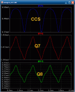
Yes , the protection device does not have a "sharp knee" ... like a zener. As shown (below 1) , it (Q9) ... starts shunting Q7 (red line) with a 1R load @ 13.5ma. At a .5R load Q9 fully becomes a "wire" (upper blue line) limiting current at 13.7ma. To reach this one would (nearly) have to short the OPS. With a different OPS this limit would also change.
Absolutely , When I build my sub amp .... A triple or LFET OPS will be mandatory.
OS
that is exactly why the peak transient current into a reactive speaker load should be allowed for. if this factor of 3 is allowed then gain droop in both the output stage and in the driver stage is incurred and in a two stage EF this puts a high current demand on the VAS. That is why I keep reminding builders that our current best BJTs can supply an 8ohm load with a two stage EF, but that lower impedance speakers require a 3stage EF to present a high impedance load to the VAS.
Absolutely , When I build my sub amp .... A triple or LFET OPS will be mandatory.
OS
Attachments
Last edited:
I think you are confirming that at 13.5mA to 13.7mA that the protection is affecting the signal being passed through.the protection device does not have a "sharp knee" ... As shown (below 1) , it (Q9) ... starts shunting Q7 (red line) with a 1R load @ 13.5ma. With a different OPS this limit would also change.
I think you are also confirming that the protection transistor starts turning on much earlier than when Vbe~600mVbe.
can you monitor what the protection transistor is doing to the signal when lower values of Vbe are applied? I.e. can you see the start of turning on at lower output current?
with a FET in either the output stage or the driver stage, beta droop becomes much less of a problem. Does Cordell tell us he prefers 3stage EF (SF) using FET output stage?.... A triple or LFET OPS will be mandatory.
Single PS....
 Nice build , anyways. 😎
You need this (Below 1)...
Look at what it does.. (below 2)
No use having a PPM amp with -70db PSRR ... 😀
OS
Attachments

- Status
- Not open for further replies.
- Home
- Amplifiers
- Solid State
- New Amplifier - ULD Extreme