In the new version Teddy Reg is not using LM317 because he said is too noisy.
An externally hosted image should be here but it was not working when we last tested it.
In the new version Teddy Reg is not using LM317 because he said is too noisy.
Thanks, that looks promising.
Any link to how to calculate the voltage regulation of the left part (Q1 through Q4)?
Simply Red, nice northern soul band. If the translucent lens has typical guts red led, no difference. What Vf you can measure across the led in operation?
1.77VSimply Red, nice northern soul band. If the translucent lens has typical guts red led, no difference. What Vf you can measure across the led in operation?
Thanks, that looks promising.
Any link to how to calculate the voltage regulation of the left part (Q1 through Q4)?
Search at his Web site Teddy Pardo home of TeddyCap TeddyXPS power supply for Naim Audio replaces HiCap and XPS "articles" "superTeddyReg"
1.77V
Looks like it has typical red led inside the transparent lens.
Hi smpkje
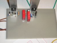
Your shunt looks awesome.... Nice and compact.... I particularly like the board.... where did you get it from ?
Your shunt looks awesome.... Nice and compact.... I particularly like the board.... where did you get it from ?
In the new version Teddy Reg is not using LM317 because he said is too noisy.
Interesting... for another take on a JFET (2N5432) + D44H11 voltage regulator see what I posted on AMB's site a few weeks ago. AMB Laboratories DIY Audio • View topic - Looking for suggestions on voltage reg circuit (scroll down and pg 2 for the depletion mosfet and JFET versions) It is a circuit I'm putting together to beef up regulation in a pair of M-Audio AV30 desktop speakers after moving the heatsink and TDA7265 chip outside on the back.
It is really not necessary to put the control loop in front of the D44H11. Since the JFET (or depletion mosfet if you use the DN2540 version) is "normally on" startup is assured and the control loop can be fed from the regulated side as I did. I used a TL431A just due to wanting to keep the parts count down, but I've put a negative rail together with a p-channel JFET (2N5462), D45H11, and a LME49860 + LT1019 reference + resistive divider for the control loop. The other half of that IC can be used with the same control loop parts (2N5432 and D44H11, of course) on the positive rail to make a control loop there to replace the TL431A, if desired.
The only change I would make now to what I posted on AMBs site is using a C-(L+R)-C filter on the front end rather than C1. The first "C" is already in the AV30, 4700uF on each rail. The L is a 2mH air core from parts express (20 gauge), the R 0.5 ohm 2W, and the final C the 10,000uF 35v cap I was going to use in the first place, which otherwise would have just been in parallel with the 4700uF. C3 should be removed as noted in the posts and some AC analysis since then yields 6.8uF as a more optimum value for C2.
For the positive rail, if using the DN2540 (either N3 or high power N5 version), the LME49860 won't work because the gate voltage is too close to the rail. That isn't a problem with the JFETs. Instead for the depletion mosfet (DN2540) use a LT1218 instead - or other favorite rail-to-rail op amp.
-agdr
Last edited:
Hi smpkje
Your shunt looks awesome.... Nice and compact.... I particularly like the board.... where did you get it from ?
Thanks. I got it from a shop here in Greece. If you like the compact connecting, take a look to PDF #3569.
Interesting... for another take on a JFET (2N5432) + D44H11 voltage regulator see what I posted on AMB's site a few weeks ago. AMB Laboratories DIY Audio • View topic - Looking for suggestions on voltage reg circuit (scroll down and pg 2 for the depletion mosfet and JFET versions) It is a circuit I'm putting together to beef up regulation in a pair of M-Audio AV30 desktop speakers after moving the heatsink and TDA7265 chip outside on the back.
It is really not necessary to put the control loop in front of the D44H11. Since the JFET (or depletion mosfet if you use the DN2540 version) is "normally on" startup is assured and the control loop can be fed from the regulated side as I did. I used a TL431A just due to wanting to keep the parts count down, but I've put a negative rail together with a p-channel JFET (2N5462), D45H11, and a LME49860 + LT1019 reference + resistive divider for the control loop. The other half of that IC can be used with the same control loop parts (2N5432 and D44H11, of course) on the positive rail to make a control loop there to replace the TL431A, if desired.
The only change I would make now to what I posted on AMBs site is using a C-(L+R)-C filter on the front end rather than C1. The first "C" is already in the AV30, 4700uF on each rail. The L is a 2mH air core from parts express (20 gauge), the R 0.5 ohm 2W, and the final C the 10,000uF 35v cap I was going to use in the first place, which otherwise would have just been in parallel with the 4700uF. C3 should be removed as noted in the posts and some AC analysis since then yields 6.8uF as a more optimum value for C2.
For the positive rail, if using the DN2540 (either N3 or high power N5 version), the LME49860 won't work because the gate voltage is too close to the rail. That isn't a problem with the JFETs. Instead for the depletion mosfet (DN2540) use a LT1218 instead - or other favorite rail-to-rail op amp.
-agdr
I can't see your schematic posted in the page 2 (You do not have the required permissions to view the files attached to this post.)
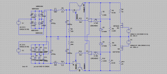
n-ch JFET + D44h11 + TL431A voltage regulator
Whoops - sorry about that - I forgot the images don't show on AMB's site unless logged in.
Here is the positive rail version with an n-channel JFET, D44H11 pass, and a TL431A error amplifier. My goal was very good regulation with a minimum of parts and a fairly low dropout, since the M-Audio AV-30s have just [ CT transformer -> full wave CT rect -> 4700uF -> TDA chip] as it sits. I was willing to sacrifice a couple of volts for regulation, which will translate into a couple of volts less to the TDA chip and a bit lower max power in return for regulation. I've updated this one with the input C-L/R-C filter and updated the gate TP (test point) voltage to reflect a 0.8A load. I've also thrown in a test load circuit that can be used to test the circuit and verify all the voltages and waveforms. You can drive that load mosfet from a function generator from 15Hz to 25kHz.
I've just spent some time looking at that Teddy Reg circuit and I can see it is essentially a gyrator on the right half, with a voltage regulator + gyrator on the left half, but no error amp loop(s). Essentially a zener(ish) feeding NPN emitter follower, with a JFET in a darlington-like config like mine, minus the zener for lower noise. The config he and I have here is almost an IGBT, but those all use enhancement FETs as far as I know. Here we are using JFETs or depletion mosfets. So essentially a do-it-yourself depletion IGBT. 😀
So a bit different design goals here. No gyrator in mine, but I did include a C-L/R-C filter upfront and mine has an error amp loop. Half the purpose of that input filter is to reduce the ripple amplitude, which is does a great job with, but also to round off the sharp corners of the ripple to make it easier for the error amp to follow. Or, to say it another way, filter out the higher frequency parts of the Fourier decomposition of the ripple waveform which has the effect of rounding corners of that waveform. Then the error amp makes a scaled down inverse version of that and feeds it to the JFET gate for cancellation. The inductor L1 isn't essential, just the resistor Rin will do a good job of forming an RC filter, but the inductor helps nuke higher order harmonics - in both directions (line [and rectifiers] to load and load back to line for injected EMI to the building wiring if you care about that).
I can see that the Teddy Reg focuses on super-low noise rather than high regulation percentages. Here I haven't measured the noise and I wouldn't believe what a spice sim is telling me on noise anyway. My focus here is more on tight line/load regulation, low dropout, and low parts count since I have to fit the whole thing on the now-external AV-30 heatsink. But I do know the noisest part will be the TL431A, but should be better than a zener (point of debate). So there is some homework for someone if they have a good sensitive wideband scope handy and build this thing - measure the baseline noise for fun! 😛
The negative rail is the same thing but with a D45H11 PNP pass, 2N5462 p-channel JFET, and the LME49860 op amp as the error amp rather than the TL431A, plus that LT1019 v reference that can be used as a sink or source. The 2N5432 is rated at 150mA, the 2N5462 at up to 16mA, and the base current of either pass transistor pulls about 11mA at .8A. So all works out. For a higher current negative regulator parallel more than one 2N5462 using appropriate (small) source resistors.
Anyway, have fun if anybody else decides to build one! 😀
-agdr
Last edited:
In an old thread member Christer measured the TL as such:
TL431 (strapped as 5V ref. using two 1kOhm resistors):
#1 @ 1mA: 3.2 3.2 3.2 3.2 3.2 uV
#1 @ 5mA: 41 41 41 41 41 uV
#1 @ 20mA: 42 42 42 42 42 uV
#2 @ 1mA: 3.2 3.3 3.2 3.3 3.3 uV
#2 @ 5mA: 41 41 41 41 41 uV
#2 @ 20mA: 42 42 42 42 42 uV
Looks like above 1mA through it kicks it up a lot. Here is what he got from a red led in same method to have an idea:
L934ID/B (red):
#1 @ 1mA: 0.29 0.28 0.28 0.27 0.28 uV
#1 @ 5mA: 0.27 0.24 0.24 0.23 0.24 uV
#1 @ 20mA: 0.39 0.32 0.29 0.48 0.29 uV
#2 @ 1mA: 0.34 0.28 0.28 0.28 0.27 uV (Vf = 1.64 V)
#2 @ 5mA: 0.24 0.24 0.25 0.24 0.25 uV (Vf = 1.72 V)
#2 @ 20mA: 0.30 0.25 0.27 0.30 0.28 uV (Vf = 1.89 V)
(Brand is Kingbright)
Yep, the Teddy Reg isn't strictly a reg as I have mentioned sometime too. Its a post filter. The ''problem'' its the irregular and relatively high Z that the filter stamps on such schemes. Did you run an open loop Bode and a Zo chart for yours BTW? It would be informative to post.
Salas: very interesting information about the TL431 noise! Thank you for posting. I'll do a search for that original thread. Looks like a fairly noisy critter.
I have the part running at a higher current than it really needs to since I originally designed the circuit to use a DN2540 depletion mosfet, which results in about a volt across R1 and R2. The JFET results in about 4 volts and hence higher TL431 current. I should re-do those resistors to lower the TL431 current which would reduce the noise a bit. BTW, that 4 volts comes from: 18V out, 18.7 on NPN base, *minus* 4.7 volts for the JFET gate. Kind of cool that the negative Vgs subtracts from the total resulting in a control voltage less than Vout.
I agree it would be very interesting to know where the poles and zeros sit, and the output impedance vs frequency. I've run some AC analysis in spice sweeping from 15hz to 25Khz, but I'm rusty enough I better spend some more time with it before I "open mouth and insert foot". 😛 Too many years since I had control system theory.
I also made a mistake on the specs for that test load voltage source I posted. I designed it with a 55 ohm resistor at a lower current. For the 22 ohm resistor and the full 0.8A current the Vsource is slightly different: Vdc bias = 1.905V, Vamplitude = 0.08V, and sweep from 15Hz to 25kHz. Also, credit where credit is due, AMB came up with that mosfet test load idea in that thread I referenced on his site. He mentioned using it for square wave transient analysis. I just modified that to generate a sine wave load.
I left an output capacitor off for a reason, to make Vout as non frequency dependent as I could. I wanted to rely on active cancellation of riipple and any residual output-current-induced voltage ripple with a fairly fast error amp loop. With C2 in to insert a small amount of phase shift into the error amp loop, the circuit seems stable up to a 200kHz sinusoidal 0.8A 18V test load and beyond. In other words, I'm relying on the amplifier being powered to be the one to limit frequency response. If someone wants to limit the frequency response looking back into the voltage regulator to insure high(er) [than audio] frequency dropoff just drop a capacitor across the output. It tests stable with a 22uF tantalum on the output. That will probably happen automatically if the audio amp parts being powered have chips with the typical 0.1uF bypass caps to ground on the supply rails.
I can see that a lot of the posters on the board here are much more current - and much more experienced with audio designs - than me. Maybe some folks can come up with ideas on dropping that TL431A noise in the circuit, either by filtering it before entering the error amp loop or actively cancelling the noise via the loop. The 100 ohm R4 is in there for the standard reason, to compensate for the negative resistance characteristic at the gate and snub oscillations. Maybe that resistor could be beefed up and a small cap to ground added to form a low pass filter, but would have to see what that would do with phase shift.
Anyway, its good enough for my AV-30 bookshelf speakers! That mod is my project with this thing. 😀
-agdr
Last edited:
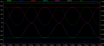
LME49860 + JFET + BJT dual rail
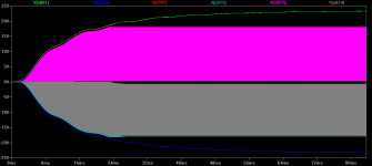
Here is a possibly lower noise version using an LME49860 op amp and LT1009 references for the control loops. The noise specs from the sheets are 6.4nV/(Hz)^1/2 for the op amp and 125nV/(Hz)^1/2 on average for the reference. NOTE! THIS ONE IS PURELY A SIMULATION unlike the TL431a version which I've built. The real circuit on this one may bear little resemblance to the sim results, so builder beware. 🙂 I'll build it over the next few weeks for fun and see how the parts match up with the math.
Simulation key:
green = unregulated pos rail voltage
blue = unregulated neg rail voltage
red = regulated positive rail
aqua = regulated negative rail
pink = positive load voltage
gray = negative load voltage
dark green = positive load current
dark blue = negative load current
The simulation is done at 25kHz since the highest frequencies are the biggest problem for stability.
Off on a computer-free vacation so I won't be able to respond to replies for awhile.
-agdr
Attachments
I'm planning on using the LV shunt reg some time down the road in a small headphone amp...
schematic is clear to me but I would be very glad when someone could point me where to find
- the basics about force-sense wiring (completely missed that 😱)
- the few calculations necessary to determine current draw
I started going through the last 100 or so posts, but 3500+ is too many...
Thanks in advance!
That is what sense/force is all about. The reg schematics recommending it are drawn also with it, all you got to do is to copy the connections in real wires.
Setting the current is Vbe/R1 for V1.2 class regs, and (Vleds-Vgs)/R1 in V1 class regs.
Setting the current is Vbe/R1 for V1.2 class regs, and (Vleds-Vgs)/R1 in V1 class regs.
- Status
- Not open for further replies.
- Home
- Amplifiers
- Power Supplies
- The simplistic Salas low voltage shunt regulator