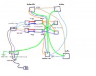
I agree. You appear to have adopted a two-star grounding system. This might make some sense if all signal level signals (clean) met at one star and all the power (dirty) signals met at the other. But instead, you've introduced a high current carrying track between the two stars - that of the speaker return current. This will compromise your decoupling (as just one bad side-effect) as the speaker current wants to return to its source, the local decouplers.
Yup. Big mistake. Thanks. 🙂
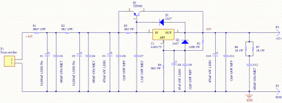
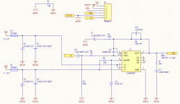
C9=100pF might be too big.
Expect a much lower value or even omit.
Connect C3 directly to C4 and tie that junction to the Power Ground.
Insert a location for a low value resistor between Signal Ground and Power Ground. You can use a resistor (1r0 to 100r) or a 0r0 link.
The Zobel and the Speaker returns must not connect to the Signal Ground.
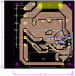
Increase the land around pin4, remove pin2 if necessary (or include pin2 in the supply trace).
Thanks for the advice and taking the time to look over this with such attention to detail.
Will add a resistor.
Will move speaker ground.
I'm going to move C4,C5 to the underside of the board to solder them directly to pins 4 and a midpoint between 1 & 5. Will take your advice and attach the ground pins of them together.
My original schematic had 11pF for C9. I can't recall why I changed it (brain aneurysm?) - a mistake.
OK, I can increase the pad width of pin 4.
your speaker ground Must not be connected with signal star ground. Speaker ground should connect straight to PS ground.
In fact you can tap the ground track going for C8 for spk gnd.
I was wondering if I'd made a mistake about speaker ground considering the amount of power going through it. Answer: yes I did. Thank for that.
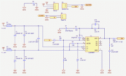
Neat design. No problems fitting a resistor behind the chip?
Last edited:
No problems fitting a resistor behind the chip?
NO. you first solder resistor and after that solderb the IC 😎. or you can also use the bottom side of pcb
Neat design. No problems fitting a resistor behind the chip?
I would bend the resistor leads to fit the resistor direct to the pins of the chip, i.e. on the top side. The resistor is attached to two long pins and these long faces are ideal for soldering a resistor to.NO. you first solder resistor and after that solderb the IC 😎. or you can also use the bottom side of pcb
I would bend the resistor leads to fit the resistor direct to the pins of the chip, i.e. on the top side. The resistor is attached to two long pins and these long faces are ideal for soldering a resistor to.

Hopefully last revision of power supply and amp PCBs. They won't win any design awards but hopefully no mistakes... *cross fingers*
Component values in non-critical areas (eg bypass capacitors) changed again due to further rummaging through parts collection.
I've bought 4 low ESR 10,000uF capacitors which will replace the array of ordinary 2200uF I was going to use.
Components shown as off the board on the Amp PCB layout are to be mounted underneath.
2x power supply board will be built and fed via 2x chassis mounted bridge rectifiers from 2x 30V transformer secondaries. They will be connected in series to get regulated 35-0-35V. The schematic isn't technically true for board 2 as, for it, GND is -35V and +35V will be GND.
I should do an interconnection schematic.
Comments and cries of horror welcome.
Attachments
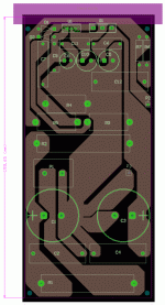
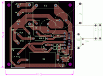
I think that pin7 should go to Power Ground.
There is a report linked from this Forum that monitored the currents coming from pin7 and they were far from quiet/constant.
If you assemble a multichannel version then you may find that Speaker Returns (both channels) are better going to the main central Star Ground.
The "on PCB" Speaker Return works, better when building a monoblock.
Last edited:
OK, thanks.I think that pin7 should go to Power Ground.
There is a report linked from this Forum that monitored the currents coming from pin7 and they were far from quiet/constant.
If you assemble a multichannel version then you may find that Speaker Returns (both channels) are better going to the main central Star Ground.
The "on PCB" Speaker Return works, better when building a monoblock.
Pin 7 moved to Power Ground (as advised in some of the first posts on this thread - was thrown because Decibel Dungeon specifies Signal Ground in gainclone guide). Various other design changes. The components in blue are attached to the bottom of the PCB.
Attachments
C3 & C4 look very big pin pitch.
A smaller pin pitch, 0.1inch or 0.2inch, should work better as HF decoupling.
A smaller pin pitch, 0.1inch or 0.2inch, should work better as HF decoupling.
100nF boxed film are usually 0.2inch pin pitch. Polypropylene are sometimes longer.:lol: OK, I'll go with more conventional 100nF MKTs. 10mm pitch instead of 22. Thanks...
They make them 0.2inch pitch for a reason, and it's not to save material costs.
I think that pin7 should go to Power Ground.
There is a report linked from this Forum that monitored the currents coming from pin7 and they were far from quiet/constant.
Are you sure that grounds leads should be connected according to "cleanliness"?
The equivalent schematic only shows grounds that belong to the input stage. That would rather qualify pin 7 as signal ground.
One could also argue that disturbances in the ground should be seen by the feedback loop, so that they can be included in the correction signal.
This from http://home.pacific.net.au/~gnb/audio/lm4780.html
The "GND" pins should be not be connected to the "Clean Earth"
Pins 12 and 19 are designated as "GND" but their function is not to set a common reference point for audio signals. Operational amplifiers with differential inputs, like the LM4780, do not require a common reference point. Establishment of a common for the input and output potentials is external to the amplifier and is usually set to the mid-point of the two power supply rails by "biasing" the differential inputs via resistive paths and providing a DC feedback path from the output. This is so that maximum voltage swing can be achieved on the output and to simplify power supply design. The amplifier internals are not actually aware, or particularly care, about how this common point is set, or its voltage in relation to the power supplies. It just amplifies the voltage difference between the inputs by the open-loop gain.
The two "GND" pins of the LM4780 are used as internal reference points for constant current sources and other signals. They draw approximately 3 milliAmps each toward the V- power supply rail. They may also carry modulation currents generated by internal amplification of the audio signal.
I haven't found many opinions on this topic beside that one. There's a brief comment in Decibel Dungeon says P7 should go to signal ground ('basic gainclone' page).Pins 12 and 19 are designated as "GND" but their function is not to set a common reference point for audio signals. Operational amplifiers with differential inputs, like the LM4780, do not require a common reference point. Establishment of a common for the input and output potentials is external to the amplifier and is usually set to the mid-point of the two power supply rails by "biasing" the differential inputs via resistive paths and providing a DC feedback path from the output. This is so that maximum voltage swing can be achieved on the output and to simplify power supply design. The amplifier internals are not actually aware, or particularly care, about how this common point is set, or its voltage in relation to the power supplies. It just amplifies the voltage difference between the inputs by the open-loop gain.
The two "GND" pins of the LM4780 are used as internal reference points for constant current sources and other signals. They draw approximately 3 milliAmps each toward the V- power supply rail. They may also carry modulation currents generated by internal amplification of the audio signal.
- The "GND" pins should be directly connected to the "star earth" point. Other connections to the "star earth" are the central 0V point of power supply, the speaker output common, the Zobel network, the power supply bypass capacitors, and the low level "clean earth" point which is used for the input signal and feedback network. The "clean earth" point is isolated by a low value resistor from the large currents which circulate through the "star earth" point.
- The "GND" pins should not be connected into the path of the "clean earth" as it will produce unwanted DC and AC interaction with this particularly sensitive part of the circuit.
EDIT: If anyone is wondering, the LM4780 consists of two 3886s in a single package.
I have some in front of me and they are indeed ~5mm.100nF boxed film are usually 0.2inch pin pitch. Polypropylene are sometimes longer.
They make them 0.2inch pitch for a reason, and it's not to save material costs.
Last edited:
I haven't found many opinions on this topic beside that one.
I'll add one here then 😀 Whilst I don't disagree with his connection of those GND pins to their own feed off the star, his circuit as shown will be susceptible to RF, reducing transparency and introducing glare. That's because his node labelled 'clean earth' is RF-polluted by being connected to a potentially long antenna - the input cable screen. Rather than adopt his wiring shown, run the RCA input ground as yet another feed from the star but keep the wire close to the input signal wire as far as possible to minimise loop area. Also far better to move the 15pF cap to the +ve input of the LM4780 to give it further RF protection.
I'll add one here then 😀 Whilst I don't disagree with his connection of those GND pins to their own feed off the star, his circuit as shown will be susceptible to RF, reducing transparency and introducing glare. That's because his node labelled 'clean earth' is RF-polluted by being connected to a potentially long antenna - the input cable screen. Rather than adopt his wiring shown, run the RCA input ground as yet another feed from the star but keep the wire close to the input signal wire as far as possible to minimise loop area. Also far better to move the 15pF cap to the +ve input of the LM4780 to give it further RF protection.
The concern was about where pin 7 GND should go on a 3886. Interesting about the potential RF problem. I thought an antenna was a conductor that had one end free-floating, but, then again, my understanding of aerials is highly incomplete, as my last cardboard and hotglue based tuned folded dipole array TV antenna project bears sad testament.
Meanwhile... Am throwing together a revised simplified main regulated PSU design with many many less superfluous low value film capacitors. Combines Roman Black's gainclone amp with a bit of Building a Gainclone chip amp with snubberized PSU.. Given the 3886's rejection ratio, it's all a bit academic. My further (unending) questions and (hopefully useful or at least entertaining) discussion on this will be relegated to the Power Supply forum. My bad in lumping them all together here.
have a look at the PSRR @ >=100kHz.Given the 3886's rejection ratio, it's all a bit academic.
Not at all good. Most discrete tend to be far better at these higher frequencies. The opamp/chipamp does very well at low frequencies.
Changed NFB and input high pass resistor values (double checking shows I made an error in previous RC calculations). NFB capacitor changed from bipolar electrolytic to polypropylene.
Hope this will be the final version...
Hope this will be the final version...
Attachments
- Status
- Not open for further replies.
- Home
- Amplifiers
- Chip Amps
- LM3886 on 1sided PCB design