Hello everybody
I have an question, Could someone give a opinion about the circuit I designed down here.
The idea came to mind when in found this beautiful To66 Japanese transistors (2SD292 NpN 13w dissipation) mounted on a heat sink.
This comes from a almost 45 year old Sony amp.
Although all the capacitors in the amp are still fine amazingly, it uses 470uf output capacitors😱 and no this is not a type error this is just awful and all the cinch connectors are corroded.
And believe me the list goes on and on.
I have build some other retro amps before (see my posts in post your solid state pics here topic).
And they where all based on the most basic LIN topology circuits, like almost every amp was in the 1960 and 1970’s.
This was and still is my hobby to build or rebuild retro things.
I used to design these simple circuits to replicate the sound as I never used to hear because I am only 22 years old.
But with these transistors I wanted to go a little step further and use current sources, and for the first time use a long taled pair as input.
I used to design circuits that had a singleton pre transistor and they where all bootstrapped current sourced.
Also this is the first schematic I designed that utilizes a dual power supply, before all my amps where based on a single supply rail with output capacitors (like the Sony amp).
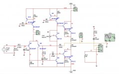
I have never done this before and this is my first try, simulations show some good results dough.
It doesn’t have to be anything super fancy or whatever since it is still based on a asymmetrical quasi complementary output pair with 45 year old slow slooww sloooowwww slooooowwwww transistors.🙄🙄
But is this circuit good enough to utilize or are there some mayor flaws here.
Or are there some minor adjustments possible to make this circuit better without using to many extra active devices.
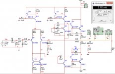
The TIP41c transistors will off-course be the Sony 2SD292 transistors and my plan was to use either BC550C and BC560C transistors in the rest of the circuit or BC337-40 and BC327-40.
For the Vas i maybe planned to use a BC141-16.
P.S. don’t mind the bias circuit this will be properly designed this was merely for simulation purposes.
Thanks guys 🙂
I will post the schematic as a picture, and I will post the Multisim simulation file in a zipped package.
And I will also post the 2SD292 datasheet.
Damn it is hard to explain things in English when you are dutch but I hope my question is clear.🙂
I have an question, Could someone give a opinion about the circuit I designed down here.
The idea came to mind when in found this beautiful To66 Japanese transistors (2SD292 NpN 13w dissipation) mounted on a heat sink.
This comes from a almost 45 year old Sony amp.
Although all the capacitors in the amp are still fine amazingly, it uses 470uf output capacitors😱 and no this is not a type error this is just awful and all the cinch connectors are corroded.
And believe me the list goes on and on.
I have build some other retro amps before (see my posts in post your solid state pics here topic).
And they where all based on the most basic LIN topology circuits, like almost every amp was in the 1960 and 1970’s.
This was and still is my hobby to build or rebuild retro things.
I used to design these simple circuits to replicate the sound as I never used to hear because I am only 22 years old.
But with these transistors I wanted to go a little step further and use current sources, and for the first time use a long taled pair as input.
I used to design circuits that had a singleton pre transistor and they where all bootstrapped current sourced.
Also this is the first schematic I designed that utilizes a dual power supply, before all my amps where based on a single supply rail with output capacitors (like the Sony amp).
I have never done this before and this is my first try, simulations show some good results dough.
It doesn’t have to be anything super fancy or whatever since it is still based on a asymmetrical quasi complementary output pair with 45 year old slow slooww sloooowwww slooooowwwww transistors.🙄🙄
But is this circuit good enough to utilize or are there some mayor flaws here.
Or are there some minor adjustments possible to make this circuit better without using to many extra active devices.
The TIP41c transistors will off-course be the Sony 2SD292 transistors and my plan was to use either BC550C and BC560C transistors in the rest of the circuit or BC337-40 and BC327-40.
For the Vas i maybe planned to use a BC141-16.
P.S. don’t mind the bias circuit this will be properly designed this was merely for simulation purposes.
Thanks guys 🙂
I will post the schematic as a picture, and I will post the Multisim simulation file in a zipped package.
And I will also post the 2SD292 datasheet.
Damn it is hard to explain things in English when you are dutch but I hope my question is clear.🙂
Attachments
Does nobody have an answer or opinion?
Is this circuit usable or does this need some modification?
Sorry for my last post but when i placed this thread to many people also replied on a thread en so my question just dissappeard is no time.
Is this circuit usable or does this need some modification?
Sorry for my last post but when i placed this thread to many people also replied on a thread en so my question just dissappeard is no time.
On the face of it, it will work. It might need a little tweaking
for thermal or frequency stability.
😎
for thermal or frequency stability.
😎
Hi
A couple of ideas:
- Add an input coupling capacitor.
- Reduce R15 and R16 to help the output transistors switch off faster.
- Use BC560B or BC560C instead of BC560A, especially for the input stage.
- Q11 and Q12 should be something with higher power rating?
The Sony amp with 470uF output capacitors sounds familiar. I think the one I had was a TA70 - it worked OK but was a horrible design!
Cheers - Godfrey
Yes it was the TA-70 man you are good🙂🙂
I want to rebuild it with the power transistors inside.
Indeed i was planning for matched BC550C and BC560c transistors in the input.
and for the driver and maybe Vas BC141-16 and BC161-16?
Input coupling cap is a good idea Thanks forgot all about that.
What value would be better for those "switch off" resistors 150-Ohm maybe?
Thanks
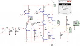
new updated schematic
Here's the new schematic with updates
And is it a good idea to make R8 a trimpot so i can adjust dc offset?
now i have about 5mv offset in simulation is this acceptable?
And the 22-Ohm emitter resistors on the long tailed pair what is there purpose i have read somewhere that these provide local feedback is this correct?
Thanks
Attachments
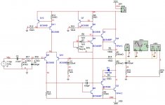
Circuit is now completed Added a diode and resistor in the bottom sziklai pair to improve symmetry.
Distortion is now 0.009% at 15 watts output power and 1 volt input.
Almost no offset voltage ( off-course in real life situations there will be differences) but I will make R14 a trimpot so I can null the offset.
So if anybody wants to use this circuit feel free to do so.
High frequency stability can be improved with adding a coil of 15-20 turns or so to the ouput tightly wound.
Here’s the new circuit and Multisim File
Greets Captain Starlog stardate April 16, 2010
Captain out………………………………….!
Attachments
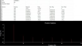
Hi Capitan,
please look at harmonics distribution,
your amp probably will sound harsh/bright/metallic/sand-like😉
Well you can keep tweaking indefinitely, but I would look to improve the DC stability.
Look at equalising the base currents into both sides of the LTP by keeping the feedback and input resistance equal, and perhaps look at adding a current mirror to the LTP to "force" equal current sharing.
Edit... making R8 adjustable... not good 🙂
Look at equalising the base currents into both sides of the LTP by keeping the feedback and input resistance equal, and perhaps look at adding a current mirror to the LTP to "force" equal current sharing.
Edit... making R8 adjustable... not good 🙂
It's looking good!
I'd take out R7. It just makes the Vbe multiplier's impedance worse. Maybe take out R16 at the input too?
I was thinking the switch-off resistors (R3 and R5) should be much lower - maybe 47 ohms. With the sim, you can check what's needed though - just look at the output transistor currents with high output at high frequency.
You're right about the emitter resistors (R22 and R23) in the input stage providing local feedback. They reduce the gain and improve the distortion of the input stage.
Now comes the interesting part:
If the amp has too much loop gain (global feedback), you might have problems with high frequency stability or oscillation.
The most obvious way to fix that is to reduce open-loop gain, so you can either increase those resistors or increase C1, however...
Increasing the resistors reduces gain and improves input-stage distortion, while increasing the capacitor reduces gain, makes input-stage distortion worse and reduces the slew rate.
So - performance can be tweaked quite nicely by fiddling with those three components.
btw, Are you keeping any of the circuitry from the TA-70? I hated the power amp section, but seem to remember the rest wasn't too bad - tone controls, phono pre-amp etc.
Cheers - Godfrey
Thanks godfrey (and others) for the input, i will fiddle with the switch-off resistors.
So increasing resistors R22-R23 is a better option then to increase C1 or should this be equal so if slightly increase R22-R23 then i should also increase C1 a little?
About what circuitry to keep from the TA-70 lets just say things got a little further than planned
I ask all these questions because i never had any education in electronics what so ever.
All my knowledge is based on, lets say 8 years of experimenting and reading books so i taught myself how to work with elctronics over the years.
But still i lack lots of theoretical knowledge that only people with many more years of experience and education can provide.
So please dont mind my "in some eyes" basic questions or mistakes
greets captain archer🙂
One more thing caught my attention... use of small signal driver transistors. At high current the outputs will suffer from loss of gain (beta droop). I think you are asking for trouble with devices rated at 100ma IC. Perhaps something like the BD139/140 etc or more modern alternatives. They may well simulate less well... be interesting to see... but the BC546 is nowhere near rugged enough.
I was thinking about using the BC141-16 BC161-16.
Thanks.
They would suit well... bit old maybe but OK for this.
These are more modern alternatives,
Attachments

Post8 showed your last revision without the LTP mirror loading.
Look at R14 & Q5 The current through R14 is VbeQ5 / R14 ~0.65/1000 = 0.65mA.
Look at R11 and Q12. The current through R11 is ~0.65/240 = 2.7mA
What is the current through Q10?
Iq10 = Ir11 - [base current of Q11 + base current of Q5 + Ir14]
= 2.7 - [0.01 + 0.05 + 0.65]
= 1.99mA
Compare Iq9 to Iq10.
Do you have a problem?
YES!!!!
The LTP collector currents must be equal at quiescent operating conditions.
Change the resistor values to balance the LTP.
At the moment there is no easy way to check that the LTP is actually balanced.
Add a pair of emitter resistors to Q9 and Q10. Just as you have in post13.
It is worth adding an emitter resistor to Q5 as well.
Add a parallel trim-pot to R11 instead.
Dissipation on Q5 is a bit high.
Look at R14 & Q5 The current through R14 is VbeQ5 / R14 ~0.65/1000 = 0.65mA.
Look at R11 and Q12. The current through R11 is ~0.65/240 = 2.7mA
What is the current through Q10?
Iq10 = Ir11 - [base current of Q11 + base current of Q5 + Ir14]
= 2.7 - [0.01 + 0.05 + 0.65]
= 1.99mA
Compare Iq9 to Iq10.
Do you have a problem?
YES!!!!
The LTP collector currents must be equal at quiescent operating conditions.
Change the resistor values to balance the LTP.
At the moment there is no easy way to check that the LTP is actually balanced.
Add a pair of emitter resistors to Q9 and Q10. Just as you have in post13.
It is worth adding an emitter resistor to Q5 as well.
no.I will make R14 a trim-pot so I can null the offset.
Add a parallel trim-pot to R11 instead.
Dissipation on Q5 is a bit high.
Last edited:
- Status
- Not open for further replies.
- Home
- Amplifiers
- Solid State
- New amp question