Looks really good, can't tell its not by an expert amp builder!
Has plenty of room for future growth, maybe to add another pair of chipamp boards. Bi-amp and active filters?
Thanks, that's very encouraging!
I was thinking it looked like a right rat's nest compared to some of the creations around here...
mund88, I'm not sure what you're referring to, I've not used stk chips in this build.
hi andy,it is a nice building!
i am very want to figure out where the slight hum from.can you take a photo of the test case?
z
I compared the star grounding shown on post 8 with the "stacked" method with a thick ground bar. Stacked gave me some very slight hum, star was silent.
i am very want to figure out where the slight hum from.can you take a photo of the test case?
z
Unfortunately I didn't take a pic of the previous earthing arrangement. It was based upon post 7 of the "Understanding star grounding thread" but with the omission of the break resistor.
It's very feasible that I wired it incorrectly!
The amp sounds good but a little laid back for my ears (the source may be contributing to this also). Any mods I could make to get a more forward presentation? Perhaps a question for another thread!
Thanks again for your input everyone.
Andy
It's very feasible that I wired it incorrectly!
The amp sounds good but a little laid back for my ears (the source may be contributing to this also). Any mods I could make to get a more forward presentation? Perhaps a question for another thread!
Thanks again for your input everyone.
Andy
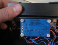
Here's the lash up in a temporary case.
I'll make things neater when I transfer the gubbins to it's permanent enclose, I promise!
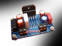
Transformer is 300VA, 25V. Pot is 100k stepped attenuator from Gigaworks.
Andy
Correct me if I am wrong here, but 100k is too high for me. I would go 25k or 50k.
Correct me if I am wrong here, but 100k is too high for me. I would go 25k or 50k.
The board seller recommended 100k so, being new to this I went with it!
What effect would you expect the the drop to 20k or 50k to make? Could the 100k be contributing to the restrained presentation I'm experiencing?
I havent seen the schematic of your chip amp nor the stepped atten, but if it uses the National reference design there is a 22K shunt resistor on the non-inverting input that should mate well with a linear 100K pot, giving it a LOG type volume curve, also for keeping the LM3886 noise within reason.
Hi,
where is the 100k Volume Control?
Where is the Power Amplifier?
What is between the Volume Control and the Power Amplifier?
where is the 100k Volume Control?
Where is the Power Amplifier?
What is between the Volume Control and the Power Amplifier?
Hi,
where is the 100k Volume Control?
Where is the Power Amplifier?
What is between the Volume Control and the Power Amplifier?
Hi Andrew,
The pot is temporarily mounted on (and isolated from) the rear panel (see post #16). Power amp boards are approx 8-10cm away, separated by air! There's nothing in between (except the connecting wires of course!)
Do I need to put more space between the pot and amp boards?
Thanks
let's assume the 200mm of twisted pair between the 100k and the Power Amp has 150pF/m
The 30pF from the cables and the 25k maximum output impedance of the 100k pot gives F(-3db) @~200kHz or about F(-1dB) @~100kHz. OK.
What are the RF filters fitted to the Power Amp and/or to the input RCA sockets?
The 30pF from the cables and the 25k maximum output impedance of the 100k pot gives F(-3db) @~200kHz or about F(-1dB) @~100kHz. OK.
What are the RF filters fitted to the Power Amp and/or to the input RCA sockets?
There are no filters on the RCA input sockets.
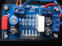
Unfortunately I don't have a schematic of the amp boards so I can't give you any info there. Would a close up picture of the boards help?
Thanks
Unfortunately I don't have a schematic of the amp boards so I can't give you any info there. Would a close up picture of the boards help?
Thanks
I'm struggling a bit to trace the track.
Are you after the four resistor values that (appear) to connect to pins 9 and 10?
Are you after the four resistor values that (appear) to connect to pins 9 and 10?
It may be easier for you to trace the circuitry from the amps input pins.
PCB pics of top and bottom will be good.
Ideally we should want the whole schematic.
PCB pics of top and bottom will be good.
Ideally we should want the whole schematic.
C5 is the input DC blocking cap (high pass filter).
There does not appear to be any RF filter capacitor location on the PCB.
It could be added easily on the back of the PCB across the Rin setting resistor.
But don't just yet. Your source impedance is too high and too variable to allow this Internal RF filter to work effectively.
Check to see which GND inputs are connected. It looks like the Signal Ground is separate from the Power Ground and Speaker Ground.
Last edited:
But don't just yet. Your source impedance is too high and too variable to allow this Internal RF filter to work effectively.
Need a better pic top shot so we can read color codes etc. no flash is best.
RF input filter can be right at the RCA jack, at least that's what pro audio gear uses i.e. ferrite bead and a small NP0 ceramic cap. If u don't have chassis shielding then at the op-amps +/- pins is second best.
Is signal INPUT GND floating, i.e. does it need to connect to off board star gnd?
looks like all 1/8 W 5% resistors are either 22K or 1K
non inverting amp input is a series 1uF +1K to pin 10 and shunt 22K to pin 10 and signal gnd (floating?)
LM3886 Gain is or 20*LOG(1+22K/1K) dB
PCB input atten 20*LOG(22/23) at higher freq > 14 Hz
total gain is +27.2-0.4 = +26.8 dB
impedance seen by wiper of switched atten. is aprox 23K to gnd
Conclusion >should be fine to use a linear 100K volume control<
shunted by 22-23K gives a LOG style atten. profile
LM3886 noise input impedance is at least 22K and is acceptable
you can use a small 100-120 pF soldered across the RCA jack for RF blocking with a ferrite bead placed on center pin for extra.
Last edited:
- Status
- Not open for further replies.
- Home
- Amplifiers
- Chip Amps
- Optimum Gainclone grounding arrangement