Hi Edmond
Thanks for the info and link. I'm a little slow catching up on EC, been busy with other stuff.😀 Since the BW of the BJT drivers is probably faster than the "stabilized" hexfet, it seems the more sensible choice, wrt complexity. I suppose the cascode is still a good improvement though, aiding in linearity. 🙂
Thanks for the info and link. I'm a little slow catching up on EC, been busy with other stuff.😀 Since the BW of the BJT drivers is probably faster than the "stabilized" hexfet, it seems the more sensible choice, wrt complexity. I suppose the cascode is still a good improvement though, aiding in linearity. 🙂
Hi
Same subject, different topic, agian.😀
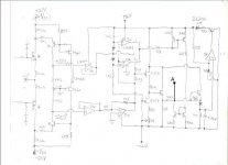
I've been pondering ways to bias the output stage based on common mode (DC) current instead of temperature. This would reduce or eliminate the 'parasitic' thermal properties of both the outputs and the error amplifiers. Also only the two outputs need to be mounted on the heatsink which simplifies hardware. Basically, it is a comparison of the positive and the negative currents. The 1K pot is a 10 turn pot that fine tunes the balance for pos/neg time on. This then goes to a limit detector which drives the 'blanking' part of the circuit. It detects when the outputs go into class B operation (actually a little before) and blanks the sample voltage. The level of current detected is translated to a voltage level, then to a controllable level shifter that sets the bias current in the outputs, and then fed through to the sample and hold circuit that drives the LED, minus the blanked 'erroneous' data sample that would be present during the class B operation. Kind of an analogue AND gate.😛
It turns out that it is important Q1 and Q2 are physically mounted together so their temperature is the same otherwise it is hard to maintain good balance with the 1K pot. If I had to choose, I would use a complementary duel package. The LED is a IL-300 infared opto-coupler. Photo-diode 1/2 is used with in the FB loop of op-amp 4/4. Photo-diode 2/2 is used to control the conductance of the Vbe multiplier that is in front of the first pre-drivers.
The 0.1 Ohm resistors are 1% power metal film resistors from Caddock. The other resistor values are written as first digit, second digit, and then multiplier. Some of these values will probably change in the end, but I put them in to give a better idea of what's going on.
ex.
100=10 Ohms
101=100 Ohms
102=1K
103=10K
ect.
This circuit seems to be promising. I still have a some tweaks to experiment with, but right now I have output bias set to 100mA that changes about +/- 15mA from very hot to the touch to cold (cooled with ice cube🙂) It still follows the positive temp co of the outputs a little, but it will not go into runaway.🙂 The implementation of the Vbe multiplier is different in this circuit than in the one I intend to use in the end and I believe this is a factor in the slight tracking inaccuracy.
Same subject, different topic, agian.😀
I've been pondering ways to bias the output stage based on common mode (DC) current instead of temperature. This would reduce or eliminate the 'parasitic' thermal properties of both the outputs and the error amplifiers. Also only the two outputs need to be mounted on the heatsink which simplifies hardware. Basically, it is a comparison of the positive and the negative currents. The 1K pot is a 10 turn pot that fine tunes the balance for pos/neg time on. This then goes to a limit detector which drives the 'blanking' part of the circuit. It detects when the outputs go into class B operation (actually a little before) and blanks the sample voltage. The level of current detected is translated to a voltage level, then to a controllable level shifter that sets the bias current in the outputs, and then fed through to the sample and hold circuit that drives the LED, minus the blanked 'erroneous' data sample that would be present during the class B operation. Kind of an analogue AND gate.😛
It turns out that it is important Q1 and Q2 are physically mounted together so their temperature is the same otherwise it is hard to maintain good balance with the 1K pot. If I had to choose, I would use a complementary duel package. The LED is a IL-300 infared opto-coupler. Photo-diode 1/2 is used with in the FB loop of op-amp 4/4. Photo-diode 2/2 is used to control the conductance of the Vbe multiplier that is in front of the first pre-drivers.
The 0.1 Ohm resistors are 1% power metal film resistors from Caddock. The other resistor values are written as first digit, second digit, and then multiplier. Some of these values will probably change in the end, but I put them in to give a better idea of what's going on.
ex.
100=10 Ohms
101=100 Ohms
102=1K
103=10K
ect.
This circuit seems to be promising. I still have a some tweaks to experiment with, but right now I have output bias set to 100mA that changes about +/- 15mA from very hot to the touch to cold (cooled with ice cube🙂) It still follows the positive temp co of the outputs a little, but it will not go into runaway.🙂 The implementation of the Vbe multiplier is different in this circuit than in the one I intend to use in the end and I believe this is a factor in the slight tracking inaccuracy.
Attachments
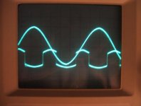
This is the waveforms for the output, 5V/div, and the voltage at point A, 10V/div. (3KHz; DC coupled) The output voltage is irrevelant becuase the blanking circuit is triggered by the current, not voltage. This is a resistive load, but if you put on a reactive load, the phase of the blanking waveform changes wrt the phase of the current.
Attachments


well, my project has been delayed by lack of employment.
anyway, in another thread mr. cordel says:
anyway, in another thread mr. cordel says:
The use of source resistors in a MOSFET output stage can sometimes help achieve a better compromize in the crossover distortion region, where transconductance droop occurs. First, the source resistors reduce somewhat the much higher transconductance exhibited by the MOSFETs at high currents outside the crossover region. Secondly, the P and N-channel MOSFETs often have somewhat different amounts of transconductance for a given amount of bias current. This can cause asymmetry in the crossover region. If slightly different values of RS are used for the P and N devices, a better balancing compromise can sometimes be achieved. We are not talking about large values of source resistance here - always less than 1 ohm. We certainly do not want to give up too much voltage swing headroom under high-current conditions.
I have to emphasize that this approach depends a lot on the individual characteristics of the P and N MOSFETs used, and does not necessarily yield really big improvements. I usually employ source resistors anyway for current monitoring and protection, so it only makes sense to tweak them for best performance if they are there anyway.
Less improvement will tend to result when better P/N matched MOSFETs are employed, like the Toshiba devices.
BTW, the addition of reasonable-sized source resistors does not usually do a lot to improve quiescent bias current matching among paralleled devices.
You can alter the output stage P/N symmetry by adjusting
the Source resistors, but I find it convenient to load the
output stage with an adjustable single-ended CCS. Works
like glue...
😎
the Source resistors, but I find it convenient to load the
output stage with an adjustable single-ended CCS. Works
like glue...
😎
Hi,
I built Upupa epops amp named DPA330. It also used Bob's Hawkford EC.
It works really great lets see:
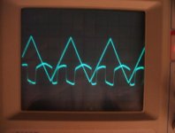
1KHz in to 4 ohms before the limitation(20V/div):

10KHz in to 4 ohms before the limitation(20V/div):

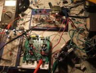
DPA 330 gets new fashion. It doesn't look like your mess:


I built Upupa epops amp named DPA330. It also used Bob's Hawkford EC.
It works really great lets see:
1KHz in to 4 ohms before the limitation(20V/div):
10KHz in to 4 ohms before the limitation(20V/div):
DPA 330 gets new fashion. It doesn't look like your mess:
Cool.🙂 It's good to see someone else using HEC with fets. It really works wonders, eh? What do the fast (100-300KHz) signals look like? Next you should try building a balanced (full bridge) amp using HEC.😉
I noticed a small difference in those outputs compared to the ones I used in mine. The hex types I used have a larger SOA, even after de-rating than 2SJ50/2SK135, and they are packaged in TO-220! However, they are not as 'linear'🙄, Vgs Th is 3.8V, and CISS & CRSS is much greater.
I noticed a small difference in those outputs compared to the ones I used in mine. The hex types I used have a larger SOA, even after de-rating than 2SJ50/2SK135, and they are packaged in TO-220! However, they are not as 'linear'🙄, Vgs Th is 3.8V, and CISS & CRSS is much greater.
You can alter the output stage P/N symmetry by adjusting
the Source resistors, but I find it convenient to load the
output stage with an adjustable single-ended CCS. Works
like glue...
😎
Hi Nelson,
Interesting approach to achieving MOSFET symmetry. I'm guessing it increases the transconductance of the device with less transconductance and vice versa. In so doing (without giving it a lot of thought), this provides a bit of crossover displacement. Does it just move the symmetry issue away from the 0 crossover? I have not though about this a lot.
The other reason I use source resistors is to reduce somewhat the high amount of transconductance that occurs in the MOSFETs at high current where they are well away from the transconductance droop zone. It is all a compromize, however.
Cheers,
Bob
Hi,
I built Upupa epops amp named DPA330. It also used Bob's Hawkford EC.
It works really great lets see:
1KHz in to 4 ohms before the limitation(20V/div):
Nice job!
Have you had a chance to measure THD yet?
Happy New Year,
Bob
Few days ago , I tried EC output stage and all I can say is that triple EF sounds superior!
I have always liked the triple EF (Locanthi T circuit) for BJT amplifier designs. Darlingtons (double EF) and two-transistor CFPs just don't have enough current gain to properly buffer the VAS, especially when driving a low-Z load.
What kind of EC design were you comparing the triple EF to? Was it a MOSFET design with EC? Was it a Darlington BJT design with EC? How good was the EC implementation? EC is more complex and requires more care and expertise in the design, especially in regard to its compensation.
Happy New Year,
Bob
I tried EC with mosfets from your article. BTW, I tried both in open loop...🙂
I have always liked the triple EF (Locanthi T circuit) for BJT amplifier designs. Darlingtons (double EF) and two-transistor CFPs just don't have enough current gain to properly buffer the VAS, especially when driving a low-Z load.
What kind of EC design were you comparing the triple EF to? Was it a MOSFET design with EC? Was it a Darlington BJT design with EC? How good was the EC implementation? EC is more complex and requires more care and expertise in the design, especially in regard to its compensation.
Happy New Year,
Bob
I have found the best way to drive Mosfets without too much complication, and because I dont like mosfets to much in class AB, for subjective reasons, they are bass light, is to use them in a triple. Two bjt stages and then mosfet outputs, preferably toshibas. Works great and is rock stable, I find it easier to stabilize than with triple with bjt, cant explain this yet though.
Ive even tried a triple and having a cfp first stage and mosfet outputs, managed to get it stable too, gives very good performance, with bjt outputs this is not possible.
I keep wondering why some designers keep using in particular vertical mosfets without a driver.
... Two bjt stages and then mosfet outputs, preferably toshibas. Works great and is rock stable, I find it easier to stabilize than with triple with bjt, cant explain this yet though.
Take a look at page 4-5 of Bob's EC mosfet amp paper😉
I have found the best way to drive Mosfets without too much complication, and because I dont like mosfets to much in class AB, for subjective reasons, they are bass light, is to use them in a triple. Two bjt stages and then mosfet outputs, preferably toshibas. Works great and is rock stable, I find it easier to stabilize than with triple with bjt, cant explain this yet though.
Ive even tried a triple and having a cfp first stage and mosfet outputs, managed to get it stable too, gives very good performance, with bjt outputs this is not possible.
I keep wondering why some designers keep using in particular vertical mosfets without a driver.
I agree. MOSFETs driven directly from a VAS, is a sub-optimal design. In my opinion, this is true whether they are Lateral or Vertical. Driving MOSFETs in a Triple configuration, where they are driven by two BJT EFs in cascade, is a good idea. If you take the EC out of my design, that is essentially what you have.
I also agree that stability of BJT Triples is not an automatic given, and can require attention to design and layout. I suspect that some otherwise good-measuring amplifiers do not sound as good as they can because their output stages are occasionally bursting into brief parasitic oscillations under certain signal conditions driving real-world loads.
Cheers,
Bob
I agree. MOSFETs driven directly from a VAS, is a sub-optimal design. In my opinion, this is true whether they are Lateral or Vertical.
don t agree with this...although buffering the vas output is benefical
in many ways, lateral mosfets from hitachi can be directly driven from
the vas output.
if the amp is carefully designed to take advantage
of this configuration, its benefits wont be limited to
its simplicity, there are more than that..
agree that it is not possible with hexfets , which require a heavier drive
current..
reagards,
wahab
- Home
- Amplifiers
- Solid State
- The Awesome Cordell Amp!