I'm interested in measuring the voltage noise of different voltage references, particularly at low frequencies, and found myself quickly running into the limitations of my audio analyzer. So, I need a preamp.
There are plenty of designs available already. To name a few, many by community members--
https://www.bartola.co.uk/valves/2014/01/18/the-noise-inspector/
http://www.janascard.cz/aHome.html
https://www.diyaudio.com/community/...card-for-audio-and-noise-measurements.342721/
I liked the idea of maintaining battery operation, allowing the circuit to float. I also wanted the option of DC coupling the inputs if needed as well as AC coupling with a very low (<0.01Hz) cutoff frequency using film caps. This led me to consider the
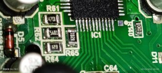
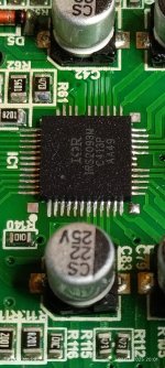
AD8428 instrumentation preamp.
The input-referrenced voltage noise is not quite as good as some of the above designs, but it's quite low and has a much lower 1/f corner than most op amps, as a $20 op amp should. ADI had the audacity to recommend
paralleling these to obtain nanovolt sensitivity. The notion of parallelling $80 worth of op amps is appalling. I'd like to try it.
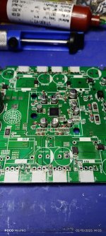
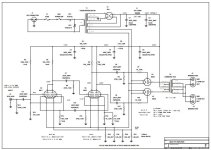
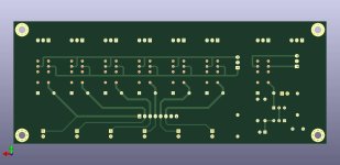
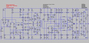
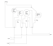
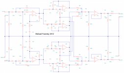
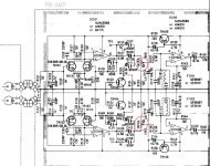
My implementation is very close to that of the datasheet. C1/C2 are input coupling caps in a footprint that accommodates up to 25uF (Kemet C4AQLBU5250M12K). With 1M resistors to bias the in-amp's inputs, fc can be made as low as 0.0064Hz. A pair of jumpers allow for DC coupling on the inputs, or connections to external capacitors to boost the input capacitance further. TI went as high as 5100uF in one
app note on measuring LDO noise, so I assume there's no harm to going big here.
F1-2, R1-2, and C3-5 provide some protection from EMI. R1-R2 does double duty and also provides protection from large differential input voltages. There is minimal protection against input voltages beyond the rails (R1/R2 provides modest current limiting for the internal diodes), so care must be taken when using DC coupling. If anyone has suggestions for which ferrite chips to use, ADI's datasheet was a bit light on details.
🙂
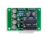
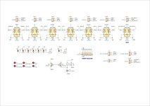
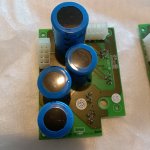
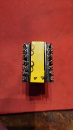
There's no great way to parallel these parts without mucking up the layout. Instead, each pin connects to a header, and daughterboards can be stacked vertically-- just like we used to do with TDA1543s. This also makes it entirely reasonable to test with just one in-amp installed, and makes the filter pins easily accessible should the need ever arise.
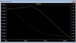
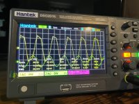
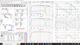
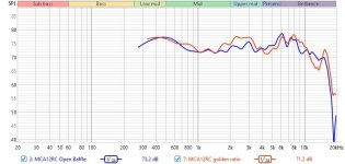
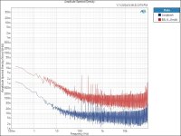
For the power supply-- I purchased a pair of EBL 9V Li-Ion batteries and was very disappointed by how noisy they are. I'm getting around 32uVRMS with a DC-90kHz bandwidth. The AD8428's 120dB+ of PSRR can no doubt handle it, but I'll sleep better at night knowing the battery is regulated. An LT3045/LT3094 pair is at least 40x quieter and provides a lower supply impedance, and makes it possible to run the preamp off of the mains if need be. I attached a measurement of the EBL battery (6F22 Li-Ion 600mAh) for reference.
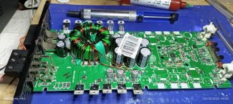
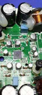
The implementation is fairly standard. Looking at the positive regulator, the battery is filtered by F3/C6. R7 sets the current limit, and R6 sets the output voltage to 7V (as the Li-Ion is closer to 8V than 9V on a full charge). C4 is the 4.7uF reference filter cap (Cset), and this board uses the recommended Murata GJ8 parts. The output cap is a kelvin-connected Panasonic SP-cap.
The board is <10cm in both directions, so should be inexpensive from the usual suppliers.
Any feedback on the design (or suggestions for potential enclosures!) would be greatly appreciated. I'm happy to make the board files available if anyone thinks it could be of use to them.