Hello.
From several month ago, i have found Class D amp for me.
Finally i arrived journey's goal.
For comparison amps, bought its from Aliexpress and ebay for 3 months,
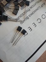
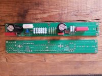
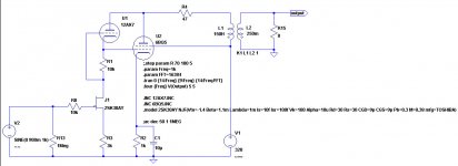
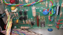
TPA3116, TDA7498, TPA3255(EVM), TAS5613, STA516B (AB32516).
First time, i bought 3116, 7498. 3116 was just bought, not use.
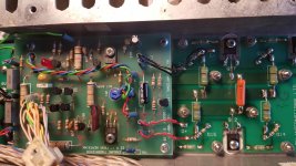
7498, It's not bad. but, when it's bass sound reached some area,
gave feeling stuffy. maybe it was caused by circuit design and Chinese
electronic parts on PCB.
Then i wanted new 7498 have well designed circuit. But, by seller's problem,
it had to changed to TAS5613. It was better than cheap 7498.
i had used 4 months, But, still not satisfied in detail.
I gathered more information about Class D amps form diyaudio.
Got information 3255, bought it. and same time EVM, too. haha.
During wait delivery, i saw post mentioned AB32512.
I interested, but, there were 3 models 32512, 32514, 32516.
32512'sound quality was verified many people.
then i wondered how about 32516 in new line up.
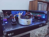
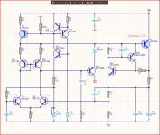
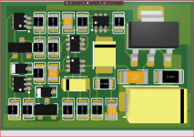
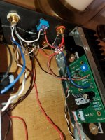
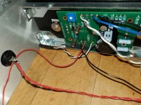
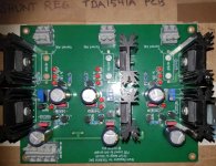
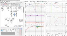
Finally, i had six amps, tested, then concluded 32516 is best in i have.
3255 was good. EVM was better than 3255 from China.
But, 3255's tone was quiet for me. Both were same.
and 32516, it was good. powerful at all range, and detailed.
In long time, i excited first time.
my speaker's output is 100W. any amps can drive it in my small room.
Compared with amps' output, it not large. it couldn't make 32516 warm.
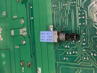
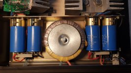
it stayed in cold. same reason, Meanwell 600SE-48 was overpowered.
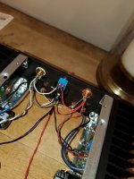
Too much fan noise, i installed fan controller, then down fan speed to lowest.
But during play music, it stayed in cold, too.
Someone interest to 32516, i recommend smaller power than expected.


