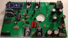
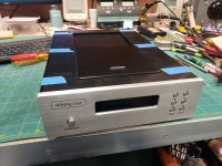
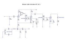
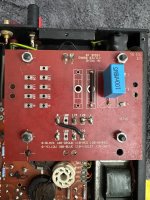
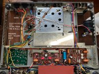
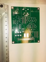
This is a group buy for the combined turntable tachometer with motor speed controller that uses the feedback from the optical sensor to keep the speed locked at 33.33 or 45 rpm. The control loop uses PID control. You can just use the board as a drop in-replacement for the Linn Valhalla board without the sensor and OLED display if you wish to solve the heat and unreliability problems of the Valhalla and just get electronic speed switching. Works fine with other turntables that use compatible synchronous motors.
The full thread discussing the development is here:
Digital Tachometer for record player (LCD display)
Features:
• Electronic switching between 33.33 rpm and 45 rpm (no more pulleys)
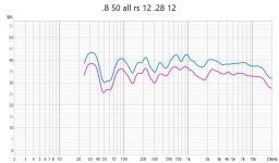
• Highly accurate sine wave frequency synthesis generated for 50Hz or 67.5Hz controlled to 0.001 Hz
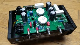
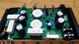
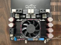
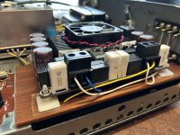
• Class A motor drive circuitry.
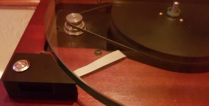
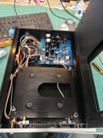
• Optional optical platter feedback sensor to lock platter rotation at exactly the right speed. This runs a PID controller loop reach maximum speed quickly then keeps rotation speed locked rock solid.
• Control over motor parameters such as frequencies, phase angle, voltage amplitude via a USB serial interface. Adjusting these values enables smoothest motor operation with minimum motor noise and vibration. Values may be written to EEPROM once optimum setup achieved.
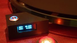
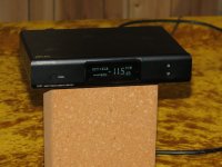
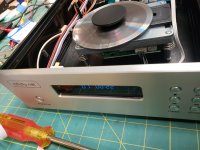
• OLED display to indicate exact platter rotation speed and WOW
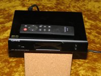
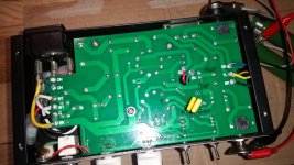
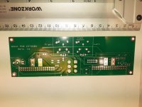
• Fits on original Linn Valhalla mounting
• Can connect to original Linn power switches.
• Speed change controlled by holding power switch for three seconds
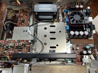
• Less heat generated than original Valhalla due to redesigned PSU section (no more burned out resistors).
• May be used for other turntables that use a two phase synchronous motor such as Airpax, Premotec, Philips e.g. Rega, Linn, Manticore, Pro-Ject etc.
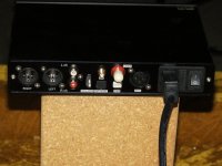
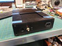
• Can be housed in a separate box.
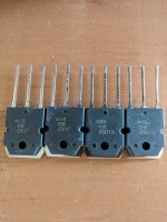
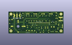
• Uses standard commonly available low cost parts such as Arduino, AD1933 DDS generators, common transistors.
There are three options:
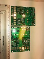
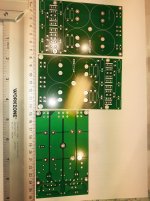
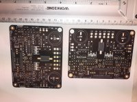
1) Bare PCB and Pre Programmed Arduino Nano 18.00 GBP
2) Full kit of parts as per attached BOM in above thread 58.00 GBP
3) Fully assembled and tested board 98.00 GBP
a) If you want the optional FFC / FPC RA header so you can use a Linn flexible circuit switch (e.g. if fitting inside a Linn LP12 replacing a Valhalla) then that's 1.00 GBP extra.
b) Recommended round momentary push switch/LED to fit OLED enclosure (see below). £4.50
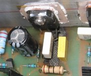
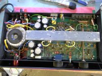
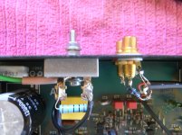
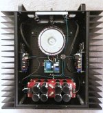
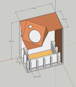
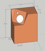
Options 2 & 3 are complete with all parts (I2C 128x32 OLED display, DDS generator PCB's, Arduino, IR detector, passives, semiconductors, heatsinks. terminal blocks etc.). All you need to add is a power switch (momentary action), indication LED and external enclosure for board (if not fitting inside TT). You will get a 3D printed box for OLED & Speed sensor. You can also use this box to mount a stop/start/speed change switch.
If you want shipping outside of UK please contact me with your address and I will work out how much extra it will be. Some examples of tracked pricing are Europe £9.35 USA £10.55 GBP
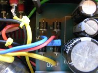
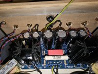
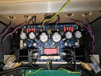
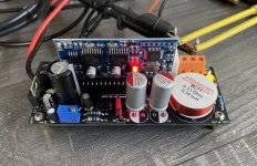
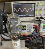
This kit contains a SMPS that is not isolated from the mains supply (similar to Linn Valhalla board). I recommend you build and test with an isolation transformer/step down transformer (100 - 240v @ 120mA) for safety of you and your test equipment. You must be confident and competent working with voltages 90V - 320V.
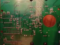
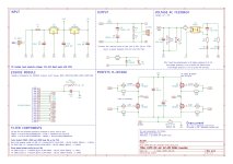
The above being said, the kit is straightforward to build and I will provide full comprehensive instructions on safety procedures, modular build and testing plus actual setup with your turntable. There are some SMD resistors to solder on the underside of the board. The most difficult part is tuning the PID parameters via serial interface/tuning application but some examples are supplied.
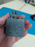
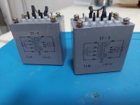
As a reminder these boards are designed to work with 2 phase synchronous motors 50Hz/60Hz that work off 6V - 110V RMS (160v p2p) that have a current consumption of approximately 10mA per phase. AKA Premotec, Airpax, Philips motors as used in Linn, Rega, Manticore, Pro-Ject and other compatible turntables Two boards can be stacked to drive 3 or 4 phase motors. You may be able to use them on shaded pole motors by using a single phase as long as the voltage and current requirements match the board specifications above. I have not tested on anything other than synchronous motors. If your motor draws more current/voltage then you will need to use an off board supplementary amplifier as per Pyramid's SG4. This motor controller can be used as a source for the sine waves and to handle the tacho & feedback/control functions.
To proceed with the group buy please add your name to each of the categories below. Please copy and paste the whole list each time you post so the list contains running additions and I don’t have to go hunting through each thread.
1) Bare PCB and Pre Programmed Arduino Nano 18.00 GBP
2) Full kit of parts 58.00 GBP
3) Fully assembled and tested board 98.00 GBP
a) Linn Valhalla switch connector option 1.00 GBP
b) Momentary action switch/LED to fit OLED enclosure 4.50GBP
 Hey! If you are here just looking for the most recent version's:


![2025-03-14 16_20_35-Rhino 7 Commercial - [Top].jpg](https://www.diyaudio.com/community/data/attachments/1343/1343123-c157b9074acd1be31f6f77d3b3cd8fa1.jpg?hash=wNBTB7vW5K "2025-03-14 16_20_35-Rhino 7 Commercial - [Top].jpg")
 - Rhino 7 Commercial -...jpg")