Leak Stereo 30 plus resistors
- By Dave 47
- Solid State
- 28 Replies
Hi,
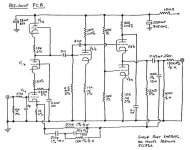
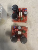
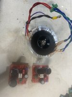
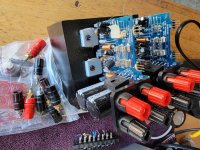
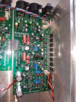
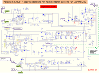
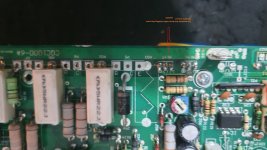
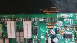
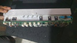
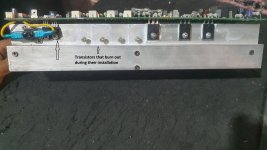
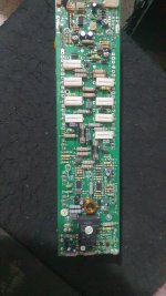
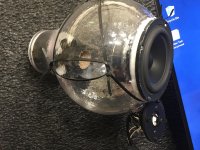
Recently acquired a Leak Stereo 30 plus with only one channel working and I find that 3 transistors are defective on the power amp board.
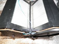
A resistor also looks suspect (burn stains around it) so I will be checking these too. Looking at the resistors I see that 5 look different from the other conventional axial lead soldered into the boards, these seem to have vertical metal tabs. Could they be wire wound? I would appreciate some advice on this please in case I need to renew some.
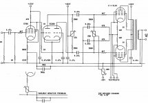
Also, does anyone know the type of resistors used on this board in addition to the ones already mentioned? The circuit diagram gives their value but not the wattage.
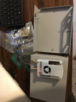
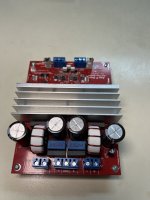
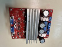
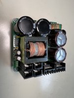
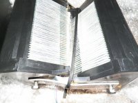
I’ve included some photos of the board which I hope will help.
Thanks,


Recently acquired a Leak Stereo 30 plus with only one channel working and I find that 3 transistors are defective on the power amp board.
A resistor also looks suspect (burn stains around it) so I will be checking these too. Looking at the resistors I see that 5 look different from the other conventional axial lead soldered into the boards, these seem to have vertical metal tabs. Could they be wire wound? I would appreciate some advice on this please in case I need to renew some.
Also, does anyone know the type of resistors used on this board in addition to the ones already mentioned? The circuit diagram gives their value but not the wattage.
I’ve included some photos of the board which I hope will help.
Thanks,

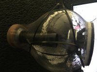

 It does appear to be all original too...