Hi Guys
Here it
sends you right away to drilling section
This will bring you direct to
assembly Section..
This will bring you to
THROUGH HOLE Section
Here a small Guideline Step by Step, how someone could create his own PCB without having a lot of Technical Knowledge, (same as me).
But before we begin here, a few things which come first.
I use BUNGARD Positive Photosensitive PCB's. There are different Manufacturers, but for me, the ones with that light blue protection sheet are the one which, seems to make the least hassles..
Precautions.:
You are working with Chemicals, so protect yourself as good as you can.
Use thin rubber gloves, use if ever possible a separate room.
Do not inhale fumes from developing solution or while etching the PCB from etching solution.
Use Clean environment.
Work in good ventilated rooms or outside on the balcony or where ever you have lots of fresh air.
RTM
Read the manual of the PCB Manufacturer and also read what can go wrong and why it goes wrong, meaning bad and not usable output..
First Comes First: ARTWORK
But first you need to create your artwork, Single side or double side makes actually not a big difference, except that if you want to make double sided PCB, the fact is if you fail on either side you have to throw away the PCB as a whole..
A few word for manufacturing:
Keep in mind that Temperatures of all the components play a big role but also surrounding temp in your room.
For German manufacturers like
Bungard, they give a lead of 20 Degrees Celsius, but not over 22 and not UNDER 20 so be exact there.
Tools you need
A Good BEAM Temp Meter where you can be sure that it measure the temp on 0.1 Degree, never mind if this is Water or Ice, Stone, Iron, Aluminum never mind the color the surface has.. ( there are cheap Temp Measuring tools out there, depending on color these will not read the correct temp.
A few plastic containers, to develop and Etch the PCB-.
Thin rubber or silicone Hand gloves.
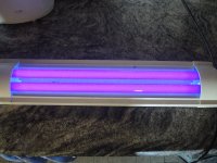
A Ultra Violet Lamp or Exposing unit. Minimum 40 Watts
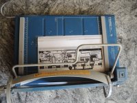
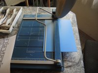
A good Paper Cutting Machine where it enables you to also cut PCB's. (check out Picture 1.6)
You need a even Surface which does not bend.
You will also need a two 3 - 5mm thick Glass Plates, large enough to cover the PCB you are going to make.
You need a Timer or Stopwatch.
You will need a certain amount of Film developing solution then also either Sodium per-sulfate. (etching Solution) Ferro chloride II 40 / 60%
A stove to heat the solution, after wards you can not use that stove for anything else again.
A lot of House hold paper..
A scissor, or sharp knife, and a lot of patience.
Then a good Gram Scale if possible Digital, because all these solutions if you mix them then it's by weight.
And there a gram does matter..
Where
A place where you can rinse the PCB after it has been finished..
Then also a place where you can dispose the used chemicals.
Do not wash it down the drain.
I have 21Pictures to show here. so I need to make 3 parts..
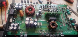
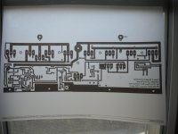
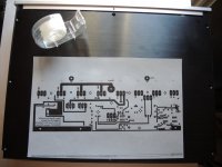
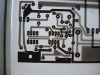
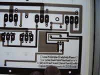
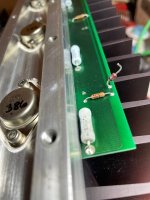
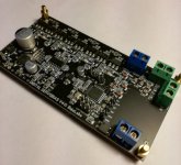
Here, the board I'm going to show, is from today.. PCB is 300x110mm double Sided..
Questions? then just ask.
Some important thing is:
Make sure that the printed side of the Artwork faces the PCB Copper side..
This counts for both the top and the bottom side, that's why it might be necessary that one side of the "Artwork Paper Film" is mirrored.
Usually I mirror the top side.
Heat up the ultra violet lamp prior to use for at least 10 minutes, make sure the lamp surface are free of dust or other none welcomed particles..
Make sure the the DEVELOPER Solution does not exceed TEMPS ABOVE 22Degrees Celsius. Neither the container where it is used in. Also check the temp of the PCB must be in the range between 20 & 22 Degrees, if it is higher then put it in the FREEZER until Temp is acceptable.
Using developer below 20 Degrees Celsius, then the film may will not be developed at all or badly, using temps above 23 and more, will give to a fast reaction to the film and the PCB will be unusable.
Check out the picture where I align, both sides of the PCB ARTWORK, using a simple Window method. Check out the Pics.
Double sided board must be made in one shot, unless you use to one sided PCB and glue them together..
The most important thing is..
THIS IS THE WAY I DO IT, and It works out that way 99% without failures..
But this does not mean that there are not other ways. I know only that way and may it come handy for the one or the other..
Thanks For reading,
Why:
JMFahey, asked me a while ago to write this,I said yes, and here I keep my promise..
Please Note:
Pictures are numbered so these are self explaining.
Proper Exposing Depending a lot on the BASIS MATERIAL
Testing is easy when using different exposure times, and then check out which one is the best.. therefore a small PCB of square inch or 2.5cm x 2,5cm is enough to find out the right Exposure time..
Proper Developing is not over 2 minutes and that is already long. usually it takes about 50 seconds.
Proper Etching can take up from 5 minutes to 1 Hour depends also on the Solution, the temp of the solution and how much the percentage the mixture contains.
Heating up the solution to 50Degrees will speed up the process quite a lot..
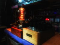
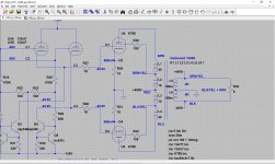
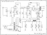
The PCB you see will be the second Prototype of the Variable Current Source Class A Amplifier which will run on Idle up to 2 watts with 0.5AMPERE only
Idle is 0.34 Ampere full load depends on the Load seen at the output. 2Ohms is children play for that AMP.
Thanks to MR. Nelson Pass, for his guidance.. and also Thanks to Mr. Rod Elliot, he, with his version of DOZ was the major Starting Point of this.
Thanks to DIY AUDIO.COM that I can be a member here..
Chris Hess


