

DIY ES9018 DAC + LM4780 AMP Details part 1
Posted 6th January 2015 at 12:30 PM by Maciej Czerwinski
DAC:
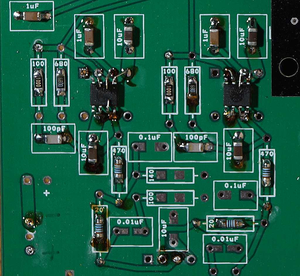
On the DIYINHK DAC board we can find ES9018 chip and ADP151 1.2V linear regulator (VDD) factory soldered. You have to populate the rest of the board yourself. I have soldered:
- ceramic and electrolytic noise filtering bypass capacitors,
- various resistors, mostly in the I/V stage,
- I/V stage op-amps (4xAD797)
- output signal low-pass filter capacitors.
The board is designed for 6 op-amps with SE output. I wanted differential output, so I have done some modifications, following the ES9018 demo board datasheet.
The I/V stage and power amp schematics (one channel):

When the main power is switched off, the relay shorts the power amp inputs in order to avoid oscillations, generated by I/V stage during discharge of its power supply bypass capacitors, to pass to the power amp.
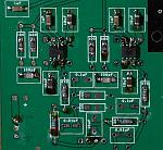
A/V stage section of the DAC board one channel, ES9018 chip side (top side in my case). I had no op-amp socket converters, so I had to improvise. You can see four blue 1k resistors of the output low-pass filter:
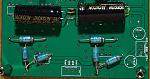
Bottom side six blue 470pF capacitors (3 per channel) of the low-pass filter and above them two 4700uF op-amp power supply bypass capacitors:
USB to I2C converter is simply an external USB computer soundcard using Cmedia CM6631 chip. It is reduced to having only I2S output and two clock signal outputs. I use 45.1584 MHz clock output to drive ES9018 clock input when playing 44.1 kHz sample rate files (1024*44.1=45.1584). The other output is 49,152 MHz, designed for 96 kHz sample rate playback (512*96=49.152). I have checked, that you can use any of the clocks, with any of the sampling rates, and the DAC sound output is always flawless.
On the DIYINHK DAC board we can find ES9018 chip and ADP151 1.2V linear regulator (VDD) factory soldered. You have to populate the rest of the board yourself. I have soldered:
- ceramic and electrolytic noise filtering bypass capacitors,
- various resistors, mostly in the I/V stage,
- I/V stage op-amps (4xAD797)
- output signal low-pass filter capacitors.
The board is designed for 6 op-amps with SE output. I wanted differential output, so I have done some modifications, following the ES9018 demo board datasheet.
The I/V stage and power amp schematics (one channel):
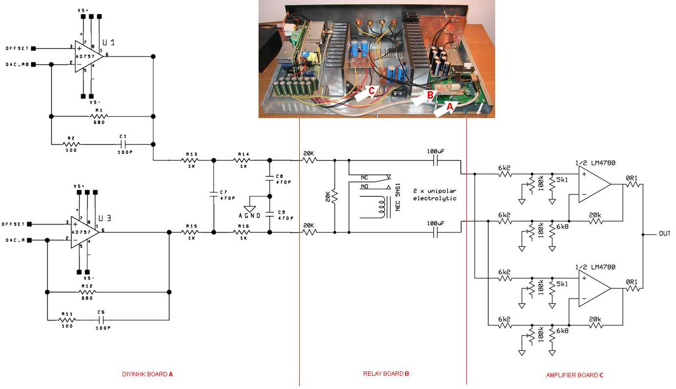
When the main power is switched off, the relay shorts the power amp inputs in order to avoid oscillations, generated by I/V stage during discharge of its power supply bypass capacitors, to pass to the power amp.
A/V stage section of the DAC board one channel, ES9018 chip side (top side in my case). I had no op-amp socket converters, so I had to improvise. You can see four blue 1k resistors of the output low-pass filter:
Bottom side six blue 470pF capacitors (3 per channel) of the low-pass filter and above them two 4700uF op-amp power supply bypass capacitors:

USB to I2C converter is simply an external USB computer soundcard using Cmedia CM6631 chip. It is reduced to having only I2S output and two clock signal outputs. I use 45.1584 MHz clock output to drive ES9018 clock input when playing 44.1 kHz sample rate files (1024*44.1=45.1584). The other output is 49,152 MHz, designed for 96 kHz sample rate playback (512*96=49.152). I have checked, that you can use any of the clocks, with any of the sampling rates, and the DAC sound output is always flawless.
Total Comments 0


