Re: Re: Re: Re: hec != hoax ?
Hi Bob,
Thanks!
Now the last hurdle, i.e. the discrepancy of the THD figures. As Jan Didden has pointed out, "the ec loop encloses only the output devices", that is, not the drivers (see: http://www.diyaudio.com/forums/showthread.php?postid=1310822#post1310822 ), I wonder whether the THD figures come closer to each other, if I manage to enclose the drivers too inside the EC loop.
Of course it'll take some time to figure that out, but I'll let you know about the results ASAP.
Cheers, Edmond.
Bob Cordell said:Very good, Edmond. Looks like we are converging. Each of us looking at what the other is doing is improving the results on both sides. That's part of what DIY is all about.
Although we don't have exactly the same distortion numbers, it does look like your results are largely confirming the kind of open-loop distortion performance of the Toshiba output MOSFETs that I have been seeing.
Cheers,
Bob [/B]
Hi Bob,
Thanks!
Now the last hurdle, i.e. the discrepancy of the THD figures. As Jan Didden has pointed out, "the ec loop encloses only the output devices", that is, not the drivers (see: http://www.diyaudio.com/forums/showthread.php?postid=1310822#post1310822 ), I wonder whether the THD figures come closer to each other, if I manage to enclose the drivers too inside the EC loop.
Of course it'll take some time to figure that out, but I'll let you know about the results ASAP.
Cheers, Edmond.
Re: Re: Re: Re: Re: Re: Re: Re: hec != hoax ?
I'm on a different track than you guys. My aim is to have an amp with EC but no global NFB. So, it's two parts, the OPS and the Vas, each with their own EC loop. The performance is not as good as your and Bob's design, but comparable to 'a pretty good poweramp' of 'classical' design. I do get two zeros after the comma for THD over most of the freq and load range.
It's playing, and now I am cleaning up de pcb and some other stuff. I'd like to publish it but have not decided where....
Jan Didden
Edmond Stuart said:Hi Jan,[snip]BTW, how about your EC output stage?
Cheers, Edmond.
I'm on a different track than you guys. My aim is to have an amp with EC but no global NFB. So, it's two parts, the OPS and the Vas, each with their own EC loop. The performance is not as good as your and Bob's design, but comparable to 'a pretty good poweramp' of 'classical' design. I do get two zeros after the comma for THD over most of the freq and load range.
It's playing, and now I am cleaning up de pcb and some other stuff. I'd like to publish it but have not decided where....
Jan Didden
2SK1530 and 2SJ201
Which reminds me: if anybody around succesfully ported the 2SK1530 and 2SJ201 models that Andy and Edmond worked on to PSpice, then I would appreciate a copy. There seem to be some obscure syntax issues which makes the netlist to error out, with nothing as error message but "expression". I tried to add {} around expressions, but it is still erroring out.
Bob Cordell said:
Yes, I think that is worth a shot.
Which reminds me: if anybody around succesfully ported the 2SK1530 and 2SJ201 models that Andy and Edmond worked on to PSpice, then I would appreciate a copy. There seem to be some obscure syntax issues which makes the netlist to error out, with nothing as error message but "expression". I tried to add {} around expressions, but it is still erroring out.
syn08 said:
Well, "very very optimistic" should be in fact "impossible". Take a look at the 4N35 datasheet. Ton is typical 2uS and max. 10uS. The signal goes in your schematic through two optocouplers. Set aside the time required to charge/discharge various capacitances and the effect of parasitic inductances, you are looking (worst case) at a response time of 20uS. After reading through the reference I quoted in my previous post, you would certainly agree that a 20uS response time is definitely not enough to protect the vertical devices against the worst case conditions (which include a beefy power supply). However, if your power supply sags under overload (contributing to the power MOSFETs current limiting, by enforcing a low di/dt ) then you (actually the MOSFETsmay get lucky and survive the short. Am I right in assuming this is the case in your setup?
You really need to go at 1uS or better response time to be on the safe side under the worst conditions. I would rather use current transformers on the PS rails instead of those slow optocouplers. Unless one may want to go for the 40nS optocouplers which is, as I said, an expensive solution.
Ovidiu,
I disagree with your conclusions on several levels here. I disagree with your interpretation of the 4N35 data sheet; I disagree about needing to kill the gate drive so quickly under short circuit conditions; I am cautious about the relevance of the article you cited.
The 4N35 is made by many manufacturers, and it is helpful to look very closely at several of the data sheets to understand its dynamic behavior. Look at both the Fairchild and Motorola data sheets.
The device comprises an IR LED emitter with about 12% efficiency in conversion to base current of the transistor. The transistor has a beta on the order of 400. Both of these are at Ic = 2 mA. The current transfer ratio (CTR) is typically 100 at IF = 10 mA. CTR is about 50 at Ic = 2 mA. The transistor is a large-area device optimized for high dc beta, and it has a Ccb of 20 pF.
Most notably, the response time for the 4N35 is specified at Ic = 2 mA, NOT IF = 2 mA. Look at the test circuit in Figure 11 and note that switching time is measured when IF is adjusted to achieve Ic = 2 mA.
This means that base current is very small, on the order of 4 uA. Now note that Miller effect of 4 uA against Ccb = 20 pF gives 0.2 V/us slew rate. Now note that with a 100 ohm load we drop 0.2 V at 2 mA, resulting in a switching time on the order of 1 us. What I am saying here is that the base current under the switching time test conditions is very small and switching time is affected by Miller effect due to the large Ccb of the large-area transistor.
Note that with a CTR = 60 at Ic = 2 mA, IF will be only about 33 uA for the switching time test. There is nothing in the data sheets that allows you to draw the conclusion that these devices are slow under conditions of high IF, which will be the case when a short circuit occurs with my protection circuit.
The Toshiba is conservatively rated at a single-pulse max peak current of 25 Amps. The IRF 240 is rated at 80 Amps repetitive with duty cycle in accordance with die temperature taking into account transient thermal impedance. IR strongly implies that failure is virtually always a thermal issue (which necessarily involves thermal time constants).
In my circuit, at 25 amps through RS = 0.22 ohms, we have about 5.5 V. After the 1.1V forward opto diode drop, we have about 4.4 V across 220 ohms for IF = 20 mA. With 12 % conversion efficiency, this will correspond to about 2.4 mA of base current. I have a 0.01 uF capacitor hanging off the base. It will take about 2 us to charge this capacitor to the turn-on Vbe of the transistor. The secondary opto couplers will probably work faster, as they have no capacitor in the base. Reaction time of my circuit will be likely less than 4 us.
The Toshiba SOA can handle 25 A for 1 ms at 55 V. No problem here.
The question that remains unresolved is how high the MOSFET current will spike in that first 4 us and whether the device in reality can handle that as a single shot isolated event.
How high it will spike depends on the driver circuit details, but it is not difficult to design the driver to roughly limit the initial current spike to some approximate high value like 25 amps. At the same time, if the current briefly spikes a lot higher than that, I seriously doubt you are going to blow a bond wire on a power device with a 10 us 100 A pulse. Ditto on die temperature. What we need here is some good old destructive testing!
The article you cited was interesting, but of questionable relevance. It was mainly in the context of switching circuits where the over-current condition was applied on a repetitive basis and the device got real hot due to repeated initial over-current intervals of several microseconds. Note that the author is almost always talking about energy loss, which translates to heat. He’s not really addressing a single-shot event and says nothing about destruction due to peak current. His over-current test circuit merely kills drive for the remainder of the clock cycle, then he hits it again, over and over.
Bottom line is that my circuit works well in practice. The photo-transistors work fast in my application (<10 us), but I don’t think they need to work that fast anyway to protect the MOSFETs in a real amplifier. My protection circuit works faster as the degree of overload gets greater. I have only used it with the IR devices that are rated for an 80-Amp spike (which really makes my circuit work fast), but I think it will do well with the Toshibas well.
Cheers,
Bob
Hi Edmond,
- Klaus
Originally posted by Edmond Stuart
Your amp seems to perform extremely well, proficiat!
The crux is bootstrapping. As you probably know, we also have used that trick in our PGP amp.
I'd actually wouldn't use bootstrapped driver supplies which are derived in any form from the main supply. I'd rather use completely independent supplies, full floating (less than 50pF Cstray is doable with a little thought). One xformer with two independent secondaries would do, for single/paralleled push-pull stage (hence two xfromers for a bridge amp -- I strongly prefer bridges when using class-A) and seperate regulated voltages for the individual drivers and cascodes can be derived from that which still could be made isolated enough from each other.
Without being picky, are you sure it's sufficient stable with the coils and without compensating caps? I guess you will soon find out when simulating the output stage with discrete components. Please let us know.
I sim'd it already with that simple discrete driver stages shown in the previous post and now I added/updated some (more or less) reasonable parasitics, still it performs quite well, had to change only little of the compensation -- Rfb and the snubber --, but well, the ss step response is far from the aperiodic ideal, and certain loads fail (which didn't when sim'd without parasitics). Also, the compensation will surely grow more complex the more I dig into the details. Inductance in the supplies is critical -- 20nH...40nH is OK, which would require a good HF layout and SOTA bypassing.
The coil parasitics are also critical, currently they are ~200uH and should have less than 20pF Cpar. The inductance itself is not a problem per se because the parallel R overides it. I set the resulting zero at 1MHz, that is about a decade lower than the bandwidth, so it doesn't add much phase shift at the point where it matters, the resistor Rfb dominates the Z at that point. Likewise, the zero from the subber/zobel is also set at 1Mhz. And then we have the infamous L//R output isolator. In general I'm aware of the stability issues of NFB designs and I know it's a long way from a succesful sim to reliable real-world circuit. And right now I'd say I'm still quite far away from a complete sucessful sim... so you are some two steps ahead of me, with the PGP, as well as the other senior designers here. I didn't do too much discrete power audio stages so far, I'm constantly learning in this exiting EE field (I'm EE)... thanks to all of you for sharing your hands-on experience!
The way you control the bias of the output devices is clever, but I'm afraid it's only feasible with class-heat, not class-AB. Did you try the latter?
This problem is quite challenging. Right now the driver's feedback goes open-loop when the current starves (and without clamping they'd kill the outputs with reverse Vbe, with the current driver supplies of +-30V). I already tried some variations along the lines of dynamic re-biasing either the whole stage or only the starving side to maintain both outputs biased at all times, but it's not easy, especially without compromising distortion, and raises stability issues -- just another feedback loop. Another thing I tried is a "fallback" AB-stage, that is, each output has it's own local class-AB complementary, biased in the conventional way (preferably the ONS ThermalTraks).
That's a point I will have to try hard (no good solution yet), as some current-on-demand scheme would be very practical to have, at least when we want to have peak output powers in the 100W++ regions. And I might allow high power peaks to be comprimised in distortion perfomance if it saved a few hundred Watts and $$$ on heatsinks etc. OTOH, a true and non-compromised class A low power design (~50W), for effcient speakers (also considering active speakers, the MF/HF sections), looks still very appealing to me if I manage it to get stable and failsafe. Or for headphone/line output stages...
PS: If you can't 'measure' the distortion with LTSpice, just use Micro-Cap.
OK, so does Micro-Cap go lower than the 0.01ppm display limit of LTSpice? That is -160dB, and I found the sine generator THD to be no better than -165dB. I ought to give it a try (and should do that anyway, to check the sims for consistency). Probably file formats and user front end are quite different, aarrgghh!
- Klaus
Bob Cordell said:
I disagree with your conclusions on several levels here.
No problem, let's agree to disagree
Although we are now up to 4uS from your original 1uS claim, I don't feel I can further discuss on this topic as long as it seems like we have a fundamental disagreement on some engineering principles.
I personally wouldn't design, build or recommend a power device protection circuit that is based on "best of the best" specs I can find (or, lacking specific data, assume) on a certain cheap critical part, allow little to no margin for worst cases, while interpreting device maximum ratings as "conservative". To me, it's like relying on a 10 degs phase margin for stability.
If your optocoupler protection circuit makes you happy, then so be it. It certainly doesn't make me happy - and unfortunately I can't afford a destructive test bench to test or prove anything further, neither can I afford to experiment something that fails the above engineering principles.
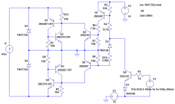
Here's a variation of Bob's switching circuit concept that uses no optos. This is just a conceptual idea - not shown is how to OR the detector outputs together to get a single trigger signal.
The zeners represent the amp's shunt reg, and ground corresponds to the amp's output node. As suggested by Bob earlier, the positive and negative sides of the shunt reg would each be shorted to the amp's output. In this case, there are two latches arranged in such a way that they can be triggered by complementary BJTs.
To simulate this in SPICE, the OFF keyword needs to be used with the latch transistors because of the bistable nature of the circuit.
Attachments
Re: Re: Re: Re: Re: hec != hoax ?
Hi Edmond,
That's a good point and I have already considered doing that by just using an extra set of emitter followers as the drivers instead of the diodes I show to get the voltages comfortably close to those that the Toshiba devices want. Not much difference between a diode and an emitter follower. The existing driver devices could then be run at a bit lower current, so the net disspation cost might not be that much. There are a couple of variations on how to do it, but that is the essence of it.
Cheers,
Bob
Edmond Stuart said:
Hi Bob,
Thanks!
Now the last hurdle, i.e. the discrepancy of the THD figures. As Jan Didden has pointed out, "the ec loop encloses only the output devices", that is, not the drivers (see: http://www.diyaudio.com/forums/showthread.php?postid=1310822#post1310822 ), I wonder whether the THD figures come closer to each other, if I manage to enclose the drivers too inside the EC loop.
Of course it'll take some time to figure that out, but I'll let you know about the results ASAP.
Cheers, Edmond.
Hi Edmond,
That's a good point and I have already considered doing that by just using an extra set of emitter followers as the drivers instead of the diodes I show to get the voltages comfortably close to those that the Toshiba devices want. Not much difference between a diode and an emitter follower. The existing driver devices could then be run at a bit lower current, so the net disspation cost might not be that much. There are a couple of variations on how to do it, but that is the essence of it.
Cheers,
Bob
KSTR said:Hi Edmond,
[snip]
OK, so does Micro-Cap go lower than the 0.01ppm display limit of LTSpice? That is -160dB, and I found the sine generator THD to be no better than -165dB. I ought to give it a try (and should do that anyway, to check the sims for consistency). Probably file formats and user front end are quite different, aarrgghh!
- Klaus
Hi Klaus,
The spurious level of Micro-Cap's sine generator plus FFT routines is about -270dB. Apparently, Micro-Cap is using double precision (64bits), while LTSpice is using only single precision (32bits), an unforgivable stupidity (i.e. false economy).
Indeed, the file format and user front end is, happily, quite different, that is, a very user friendly interface and one single file that also contains the relevant models.
Cheers, Edmond.
syn08 said:
No problem, let's agree to disagree
Although we are now up to 4uS from your original 1uS claim, I don't feel I can further discuss on this topic as long as it seems like we have a fundamental disagreement on some engineering principles.
I personally wouldn't design, build or recommend a power device protection circuit that is based on "best of the best" specs I can find (or, lacking specific data, assume) on a certain cheap critical part, allow little to no margin for worst cases, while interpreting device maximum ratings as "conservative". To me, it's like relying on a 10 degs phase margin for stability.
If your optocoupler protection circuit makes you happy, then so be it. It certainly doesn't make me happy - and unfortunately I can't afford a destructive test bench to test or prove anything further, neither can I afford to experiment something that fails the above engineering principles.
Hi Ovidiu,
Yes, we do certainly disagree. My original 1 us number was just an uninformed guess, and the 4 us is certainly not hard to hit and does not even remotely depend on the "best of the best" of opto-couplers. BTW, the basic scheme can be implemented without the niceties of opto-couplers just by using all transistors floating with the signals if you don't trust the speed of the opto-couplers.
Our biggest, most important disagreement does not have to do with the speed of the optocouplers. It has to do with how long the MOSFET can survive an over-current condition resulting from a short circuit. I believe that, given reasonable driver design that does not allow extreme overcurrents, the MOSFETs will easily endure 100 us.
Maybe I'll do some destructive testing after Thanksgiving to prove it to you. We both agree that protection is important, and I assure you that I firmly believe it must be just as reliable as you. I do not believe in taking unnecessary risks when it comes to protection. My scheme has already saved me from losing output devices a number of times.
By the way, how do you know that laterals will survive in any design without short circuit protection 100% of the time under worst-case conditions?
Cheers,
Bob
andy_c said:Here's a variation of Bob's switching circuit concept that uses no optos. This is just a conceptual idea - not shown is how to OR the detector outputs together to get a single trigger signal.
The zeners represent the amp's shunt reg, and ground corresponds to the amp's output node. As suggested by Bob earlier, the positive and negative sides of the shunt reg would each be shorted to the amp's output. In this case, there are two latches arranged in such a way that they can be triggered by complementary BJTs.
To simulate this in SPICE, the OFF keyword needs to be used with the latch transistors because of the bistable nature of the circuit.
Hi Andy,
Cool! I've also wondered about doing it with some kind of arrangement using triacs, but have not done it.
Cheers,
Bob
Re: 2SK1530 and 2SJ201
Never mind, I figured it out:
.SUBCKT 2SJ201 1 2 3
* Node 1 -> Drain
* Node 2 -> Gate
* Node 3 -> Source
***************************
.PARAM pi=3.1416
.PARAM Cgdmin=143p
.PARAM Cgdmax=2677p
.PARAM a=0.31548599
.PARAM B={(Cgdmin + 0.5 * pi * Cgdmax) / (1 + 0.5 * pi)}
.PARAM C={(Cgdmax - Cgdmin) / (1 + 0.5 * pi)}
M1 4 5 3 3 PMOS5
RG 2 5 1m
RD 1 4 1m
;RD 1 4 0.198
DDS 1 3 DDS
CGS 5 3 1414p
GGD 2 1 VALUE={ if( V(2,1) < 0, {-C * tanh( a * V(2,1) ) + B}, {-C * atan( a * V(2,1) ) + B} ) * DDT(V(2,1)) }
.MODEL PMOS5 PMOS ( LEVEL=5 L=2U W=0.5m
;+ EKVINT = 1
+ cox = 3.6e-4
+ xj = 2e-7
+ vto= -1.72 ; threshold voltage, adjust this value at will
+ gamma=6
+ phi=2.4
+ kp=8.5e-2
+ e0=2.0e+11
+ ucrit=2.67e+13
+ dl=0 dw=0
+ lambda=1.1305e5
+ ibn=1.0 iba=0 ibb=3.0e8
+ weta=0.0 q0=0 LK=2.9e-7
+ leta=0.0 rsh=0.0 )
**********************************************************************
.MODEL DDS D( N=1.55178 IS=2e-8 RS=0.01 CJO=1544p M=0.4786242 VJ=0.423139 BV=200 )
**********************************************************************
.ENDS
.SUBCKT 2SK1530 1 2 3
* Node 1 -> Drain
* Node 2 -> Gate
* Node 3 -> Source
***************************
.PARAM pi=3.1416
.PARAM Cgdmin=42.8114p
.PARAM Cgdmax=1216.887p
.PARAM a=0.31548599
.PARAM B={(Cgdmin + 0.5 * pi * Cgdmax) / (1 + 0.5 * pi)}
.PARAM C={(Cgdmax - Cgdmin) / (1 + 0.5 * pi)}
M1 4 5 3 3 NMOS5
RG 2 5 1m
RD 1 4 383m
DDS 3 1 DDS
CGS 5 3 850p
GGD 2 1 VALUE={ if( V(2,1) > 0, {C * tanh( a * V(2,1) ) + B}, {C * atan( a * V(2,1) ) + B} ) * DDT(V(2,1)) }
.MODEL NMOS5 NMOS (LEVEL=5 L=2U W=0.5m
;+ EKVINT = 1
+ cox = 7e-4
+ xj = 1e-8
+ vto=1.97 gamma=5.9999694 phi=3.4298218
+ kp=7.95e-2
+ e0=2.0568449051e+11
+ ucrit=2.6680517254825e+13
+ dl=0 dw = 0
+ lambda=1.1305e5
+ ibn=1.0 iba=0 ibb=3.0e8
+ weta=0.0 q0=0 LK=2.9e-7
+ leta=0.0 rsh=0.0 )
****************************************************************************
.MODEL DDS D ( N=1.5517725590608 IS=2e-8 RS=0.009989 CJO=405.936p M=0.560182 VJ=2.403248 )
****************************************************************************
.ENDS
syn08 said:
if anybody around succesfully ported the 2SK1530 and 2SJ201 models that Andy and Edmond worked on to PSpice, then I would appreciate a copy.
Never mind, I figured it out:
.SUBCKT 2SJ201 1 2 3
* Node 1 -> Drain
* Node 2 -> Gate
* Node 3 -> Source
***************************
.PARAM pi=3.1416
.PARAM Cgdmin=143p
.PARAM Cgdmax=2677p
.PARAM a=0.31548599
.PARAM B={(Cgdmin + 0.5 * pi * Cgdmax) / (1 + 0.5 * pi)}
.PARAM C={(Cgdmax - Cgdmin) / (1 + 0.5 * pi)}
M1 4 5 3 3 PMOS5
RG 2 5 1m
RD 1 4 1m
;RD 1 4 0.198
DDS 1 3 DDS
CGS 5 3 1414p
GGD 2 1 VALUE={ if( V(2,1) < 0, {-C * tanh( a * V(2,1) ) + B}, {-C * atan( a * V(2,1) ) + B} ) * DDT(V(2,1)) }
.MODEL PMOS5 PMOS ( LEVEL=5 L=2U W=0.5m
;+ EKVINT = 1
+ cox = 3.6e-4
+ xj = 2e-7
+ vto= -1.72 ; threshold voltage, adjust this value at will
+ gamma=6
+ phi=2.4
+ kp=8.5e-2
+ e0=2.0e+11
+ ucrit=2.67e+13
+ dl=0 dw=0
+ lambda=1.1305e5
+ ibn=1.0 iba=0 ibb=3.0e8
+ weta=0.0 q0=0 LK=2.9e-7
+ leta=0.0 rsh=0.0 )
**********************************************************************
.MODEL DDS D( N=1.55178 IS=2e-8 RS=0.01 CJO=1544p M=0.4786242 VJ=0.423139 BV=200 )
**********************************************************************
.ENDS
.SUBCKT 2SK1530 1 2 3
* Node 1 -> Drain
* Node 2 -> Gate
* Node 3 -> Source
***************************
.PARAM pi=3.1416
.PARAM Cgdmin=42.8114p
.PARAM Cgdmax=1216.887p
.PARAM a=0.31548599
.PARAM B={(Cgdmin + 0.5 * pi * Cgdmax) / (1 + 0.5 * pi)}
.PARAM C={(Cgdmax - Cgdmin) / (1 + 0.5 * pi)}
M1 4 5 3 3 NMOS5
RG 2 5 1m
RD 1 4 383m
DDS 3 1 DDS
CGS 5 3 850p
GGD 2 1 VALUE={ if( V(2,1) > 0, {C * tanh( a * V(2,1) ) + B}, {C * atan( a * V(2,1) ) + B} ) * DDT(V(2,1)) }
.MODEL NMOS5 NMOS (LEVEL=5 L=2U W=0.5m
;+ EKVINT = 1
+ cox = 7e-4
+ xj = 1e-8
+ vto=1.97 gamma=5.9999694 phi=3.4298218
+ kp=7.95e-2
+ e0=2.0568449051e+11
+ ucrit=2.6680517254825e+13
+ dl=0 dw = 0
+ lambda=1.1305e5
+ ibn=1.0 iba=0 ibb=3.0e8
+ weta=0.0 q0=0 LK=2.9e-7
+ leta=0.0 rsh=0.0 )
****************************************************************************
.MODEL DDS D ( N=1.5517725590608 IS=2e-8 RS=0.009989 CJO=405.936p M=0.560182 VJ=2.403248 )
****************************************************************************
.ENDS
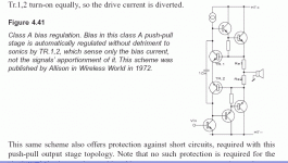
Regarding my output stage idea, this morning I now see something that uses the same concept, a feedback loop that just holds the added voltage drop across both output emitter resistors constant. Nobody less than Bruno "UcD" Putzeys designed it (together with Sander Sassen), a really straight design:
http://www.diyaudio.com/forums/showthread.php?threadid=96853
I need to study that in detail.
And like I intend to do, they did it as a bridge design which I think is only of true benefit with class A.
Seems I'm not on a completely false track...
- Klaus
http://www.diyaudio.com/forums/showthread.php?threadid=96853
I need to study that in detail.
And like I intend to do, they did it as a bridge design which I think is only of true benefit with class A.
Seems I'm not on a completely false track...
- Klaus
KSTR said:Regarding my output stage idea, this morning I now see something that uses the same concept, a feedback loop that just holds the added voltage drop across both output emitter resistors constant. Nobody less than Bruno "UcD" Putzeys designed it (together with Sander Sassen), a really straight design:
http://www.diyaudio.com/forums/showthread.php?threadid=96853
Hi Klaus,
that particular idea is quite old and was published by Allison in 1972 according to Ben Duncan's book:
Cheers
Alex
Attachments
KSTR said:Regarding my output stage idea, this morning I now see something that uses the same concept, a feedback loop that just holds the added voltage drop across both output emitter resistors constant. Nobody less than Bruno "UcD" Putzeys designed it (together with Sander Sassen), a really straight design:
http://www.diyaudio.com/forums/showthread.php?threadid=96853
[snip]
- Klaus
Hi Klaus,
Also have a look at: E.M. Cherry, "A high quality audio power amplifier" in Monitor Porc. IREE Aust., Jan/Feb 1978, pp 1-8,
and referred at in Electronics World, June 1997, p. 476.
Cheers, Edmond.
Re: Re: Re: Re: Re: Re: hec != hoax ?
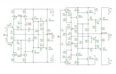
Hi Bob,
See below how I've eliminated the distortion of the drivers. Admittedly, it's a quick and dirty solution by using CFP stages and current sources, but nevertheless it gives optimal results.
Also notice that I've slightly adjusted the compensating caps so that the NFB loop in both circuits has the same Ft, 2.8MHz.
For results, see next post.
Cheers, Edmond.
Hi Edmond,
That's a good point and I have already considered doing that by just using an extra set of emitter followers as the drivers instead of the diodes I show to get the voltages comfortably close to those that the Toshiba devices want. Not much difference between a diode and an emitter follower. The existing driver devices could then be run at a bit lower current, so the net disspation cost might not be that much. There are a couple of variations on how to do it, but that is the essence of it.
Cheers,
Bob
Hi Bob,
See below how I've eliminated the distortion of the drivers. Admittedly, it's a quick and dirty solution by using CFP stages and current sources, but nevertheless it gives optimal results.
Also notice that I've slightly adjusted the compensating caps so that the NFB loop in both circuits has the same Ft, 2.8MHz.
For results, see next post.
Cheers, Edmond.
Attachments
hec != hoax ?
(continuation)
The THD20 in ppm at various power levels into 8 Ohm
1.0W : HEC: 22.28 NFB: 22.17
10 W : HEC: 54.55 NFB: 54.88
100W: HEC: 60.27 NFB: 54.00
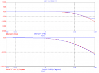
As one can see, not only the THD figures are almost identical, but also the gain and phase plots of both amplifiers (see below) closely match each other.
I hope that these figures provide enough evidence that HEC is nothing more (or less) than NFB in disguise.
Cheers, Edmond.
(continuation)
The THD20 in ppm at various power levels into 8 Ohm
1.0W : HEC: 22.28 NFB: 22.17
10 W : HEC: 54.55 NFB: 54.88
100W: HEC: 60.27 NFB: 54.00
As one can see, not only the THD figures are almost identical, but also the gain and phase plots of both amplifiers (see below) closely match each other.
I hope that these figures provide enough evidence that HEC is nothing more (or less) than NFB in disguise.
Cheers, Edmond.
Attachments
Re: hec != hoax ?
Hmmm. Too good to be true, almost. Could it be that what is limiting the THD levels in each case, is what the two versions have in common - i.e. the input emitter followers (Q2,3, Q20,21)? These are outside the hec loop as well as the nfb loop if I'm not mistaken.
Jan Didden
Edmond Stuart said:(continuation)
The THD20 in ppm at various power levels into 8 Ohm
1.0W : HEC: 22.28 NFB: 22.17
10 W : HEC: 54.55 NFB: 54.88
100W: HEC: 60.27 NFB: 54.00
As one can see, not only the THD figures are almost identical, but also the gain and phase plots of both amplifiers (see below) closely match each other.
I hope that these figures provide enough evidence that HEC is nothing more (or less) than NFB in disguise.
Cheers, Edmond.
Hmmm. Too good to be true, almost. Could it be that what is limiting the THD levels in each case, is what the two versions have in common - i.e. the input emitter followers (Q2,3, Q20,21)? These are outside the hec loop as well as the nfb loop if I'm not mistaken.
Jan Didden
hec != hoax ?
Hi Lumanauw,
The input and output impedance are frequency dependent, so I hope you don't mind that I'll show you them at only 20kHz.
Zi HEC: 2.17MOhm, NFB: 1.97MOhm.
Zo HEC: 3.3mOhm, NFB: 3.6mOhm.
At all other frequencies they are also almost identical.
Cheers, Edmond.
lumanauw said:Hi, Edmond,
Very interesting
Hi Lumanauw,
The input and output impedance are frequency dependent, so I hope you don't mind that I'll show you them at only 20kHz.
Zi HEC: 2.17MOhm, NFB: 1.97MOhm.
Zo HEC: 3.3mOhm, NFB: 3.6mOhm.
At all other frequencies they are also almost identical.
Cheers, Edmond.
- Home
- Amplifiers
- Solid State
- Bob Cordell Interview: Error Correction