Re: Re: Re: hec != hoax ?
Very good, Edmond. Looks like we are converging. Each of us looking at what the other is doing is improving the results on both sides. That's part of what DIY is all about.
Although we don't have exactly the same distortion numbers, it does look like your results are largely confirming the kind of open-loop distortion performance of the Toshiba output MOSFETs that I have been seeing.
Cheers,
Bob
Edmond Stuart said:
Hi Bob,
Now the gain and phase plots look completely different. For example, the 1dB gain bubble has gone and the phase shift is far less due to the smaller gate stoppers. Interestingly, when I remove the compensating cap C10 (39pF) in your original schematic, your OPS also has a small gain bubble (0.5dB at 3MHz).
In order to create a playing level field, I've used the same transistors in your OPS as in mine, so the fast 2SC3601/2SA1407 as driver and for all other BJTs 2N5401/2N5551. The 95pF compensating caps might look funny, but at this value the Ft of the NFB loop gain is exactly the same as in your OPS. Needless to say that the gate stopper stuff is also identical.
The phase lag at 10 MHz has improved from 70 to 40 degrees and, if you don't mind, it is even slightly better than HEC.
And the distortion, HEC: THD20=70ppm, NFB: 55ppm (BW=200kHz).
Cheers, Edmond.
NB: red = HEC, blue = NFB.
Very good, Edmond. Looks like we are converging. Each of us looking at what the other is doing is improving the results on both sides. That's part of what DIY is all about.
Although we don't have exactly the same distortion numbers, it does look like your results are largely confirming the kind of open-loop distortion performance of the Toshiba output MOSFETs that I have been seeing.
Cheers,
Bob
G.Kleinschmidt said:
187W into 4 ohms = 38.7V peak. With three pairs of output devices, this works out to 3.225A peak per device pair.
Bob writes:
Performance of that very same simulation at 40V peak at 20 kHz into 8 ohms is as follows:
Without EC: THD-20 = 0.185 %
Then speculates that the gap between your figures and his figures may be due to:
.....the 4-ohm condition (if you are using a single pair at 150 mA), combined with the poor performance of the laterals may largely explain it.
Like, HELLLLOOOOOOOO!!!!
The gap is due to a BS simulation. For a start, 40V driving 8 ohms = 5A peak for his single pair of devices - so his THD-20 figure comes from a MOSFET output stage actually driven harder than yours.
Secondly, 0.185% THD-20 under these conditions is obviously from a simulator because it sure as fudge doesn't correspond to realistic real world figures. Bob is well aware of this, as 0.185% THD-20 isn't anywhere near what he reported in his EC MOSFET amp paper, where he quotes a measured non-EC THD-20 in the same same league with his vertical MOSFET OPS as you do with your lateral MOSFET OPS.
Hi Glen.
You're wrong. Look at the subsequent posts, including my answer above to your earlier very reasonable point. Too bad you didn't wait for that answer. You destroy your own credibility with shoot-from-the-hip posts like this.
Cheers,
Bob
Bob Cordell said:
Hi Ovidiu,
Could you elaborate on the opto coupler speed issue? In my protection circuit, the optocouplers are quite fast, as the sensor is a silicon transistor structure. Probably on the order of 1 us or better. Are you suggesting that a 1 us response time to shut off the gate drive to the MOSFETs is not fast enough in the event of a short circuit?
Thanks,
Bob
Bob,
1uS response time for that circuit, using regular optocouplers is very, very optimistic.
Take a look here http://powerelectronics.com/power_semiconductors/power_mosfets/power_protecting_mosfets_against/ for a good analysis on how a mosfet protection should work and what are the criteria to design an efficient protection schema. Its not as simple as "shut it down fast".
Klaus wrote:
I like it or rather I like the sheer audacity of it.
Whether or not this circuit can be tamed in practice to avert it form causing a permanent tear in the space-time continuum is another matter entirely, but I like your ideas Klaus. You are using BJTs for a high speed circuit, you are using ICs designed for an entirely different application and you have won me over completely by daring to use discrete inductors in the fb path. Nice.
ahem, it's 20Vp into 8ohms//50nF (clip limit is 5.5ohms), so it's only 25W with a 20Vp sine.
But the THD numbers are true... believe me, I really hesitate to believe it as well, mainly because the op-amp models all state "distortion not characterisized" (that's why I need to sim it with discretes, and build it). But, in fact when I sim the op-amps as simple followers with no load and 2Vp drive, I get more distortion from the op-amps alone! I tried THS6012+MJL3181/1302 and AD811+MJE15032/33. OTOH the op-amps run at optimal conditions: no common mode voltage and only little output swing, less than 300mV for the shown circuit. Also, the cascoding helped a lot. The stage is virtually isolated from the drive/output voltage, it only "sees" output current. Of course the design is not finished at any rate (not procection of any kind, won't like >0.5uF at the output), it's only a study so far...but the stunning numbers make me think I give i try, instead of fiddling around with chip amps biased to class A by the same method (which is how I came across the whole thing).
I like it
or rather I like the sheer audacity of it. Whether or not this circuit can be tamed in practice to avert it form causing a permanent tear in the space-time continuum is another matter entirely, but I like your ideas Klaus. You are using BJTs for a high speed circuit, you are using ICs designed for an entirely different application and you have won me over completely by daring to use discrete inductors in the fb path. Nice.
Bob Cordell said:
Hi Glen.
You're wrong. Look at the subsequent posts, including my answer above to your earlier very reasonable point. Too bad you didn't wait for that answer. You destroy your own credibility with shoot-from-the-hip posts like this.
Cheers,
Bob
Well I'm glad that my earlier point was very reasonable and has led to further clarification on your part, but no, I do not think that my credibility is destroyed or that you have demonstrated that I am wrong.
To reiterate, I contend that the gulf between your 0.185% THD-20 and Syn08's 1.1% THD-20 is obviously not due to the "4 ohm condition" (your single MOSFET pair is actually being driven harder with 8 ohms than Syn08's 3 pairs are with 4 ohms) nor necessarily entirely due to the use of lateral MOSFETs over vertical MOSFETs.
Your 0.185% THD-20 comes from a simulator. Right?
Syno8's 1.1% THD-20 comes from a THD analyser connected to a real OPS. Right?
Hi Glen,
Comments like ...
Please attempt to keep your posts on a professional level. I also don't think you have made your point well either, so settle down please.
-Chris
Comments like ...
Show a lack of respect on your part to other members, everyone who reads this kind of thing and especially your target. Now that type of thing does harm your credibility.The gap is due to a BS simulation.
Please attempt to keep your posts on a professional level. I also don't think you have made your point well either, so settle down please.
-Chris
anatech said:Hi Glen,
Comments like ...
Show a lack of respect on your part to other members, everyone who reads this kind of thing and especially your target. Now that type of thing does harm your credibility.
Please attempt to keep your posts on a professional level. I also don't think you have made your point well either, so settle down please.
-Chris
Thanks very much, Chris. I'll pass on responding to Glen so that we all can focus on the technical merits of our discussions.
Best regards,
Bob
syn08 said:
1uS response time for that circuit, using regular optocouplers is very, very optimistic.
Well, "very very optimistic" should be in fact "impossible". Take a look at the 4N35 datasheet. Ton is typical 2uS and max. 10uS. The signal goes in your schematic through two optocouplers. Set aside the time required to charge/discharge various capacitances and the effect of parasitic inductances, you are looking (worst case) at a response time of 20uS. After reading through the reference I quoted in my previous post, you would certainly agree that a 20uS response time is definitely not enough to protect the vertical devices against the worst case conditions (which include a beefy power supply). However, if your power supply sags under overload (contributing to the power MOSFETs current limiting, by enforcing a low di/dt ) then you (actually the MOSFETs
may get lucky and survive the short. Am I right in assuming this is the case in your setup?You really need to go at 1uS or better response time to be on the safe side under the worst conditions. I would rather use current transformers on the PS rails instead of those slow optocouplers. Unless one may want to go for the 40nS optocouplers which is, as I said, an expensive solution.
syn08 said:
Well, "very very optimistic" should be in fact "impossible". Take a look at the 4N35 datasheet. Ton is typical 2uS and max. 10uS. The signal goes in your schematic through two optocouplers. Set aside the time required to charge/discharge various capacitances and the effect of parasitic inductances, you are looking (worst case) at a response time of 20uS. After reading through the reference I quoted in my previous post, you would certainly agree that a 20uS response time is definitely not enough to protect the vertical devices against the worst case conditions (which include a beefy power supply). However, if your power supply sags under overload (contributing to the power MOSFETs current limiting, by enforcing a low di/dt ) then you (actually the MOSFETs
You really need to go at 1uS or better response time to be on the safe side under the worst conditions. I would rather use current transformers on the PS rails instead of those slow optocouplers. Unless one may want to go for the 40nS optocouplers which is, as I said, an expensive solution.
One option would be to use a crude, but fast acting BJT current clamp on the OPS, set to say 1.5 - 2 times the optocoupler trigger current. That way the short circuit current can be limited to a safe level during the time it takes for the protection circuitry to shut the amplifier down.
Cheers,
Glen
Re: Re: Re: Re: Re: hec != hoax ?
Edmond:
Take a look at the OPA633 simplified schematic: http://focus.ti.com/lit/ds/symlink/opa633.pdf
While certainly not identical with yours, there are some similarities. This high speed buffer design may suggest an even better way to build an OPS with local NFB.
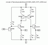
Originally posted by Edmond Stuart
Here is already the schematic:
Edmond:
Take a look at the OPA633 simplified schematic: http://focus.ti.com/lit/ds/symlink/opa633.pdf
While certainly not identical with yours, there are some similarities. This high speed buffer design may suggest an even better way to build an OPS with local NFB.
Hi Ovidiu,
It's pretty funny how many times I've looked at that buffer and didn't get how it applies to what I'm doing. Duh! There is the answer to limiting current. It is one of the last things I think about in a design - but I still should have recognized this.
-Chris
It's pretty funny how many times I've looked at that buffer and didn't get how it applies to what I'm doing. Duh!
There is the answer to limiting current. It is one of the last things I think about in a design - but I still should have recognized this.-Chris
anatech said:Hi Ovidiu,
It's pretty funny how many times I've looked at that buffer and didn't get how it applies to what I'm doing. Duh!
Hi Chris,
That's not a current limiter. It's actually a "current supercharger". When the difference between input and output voltage becomes large enough, one of the inner devices will turn on, supplying an increased base current to the appropriate output device, allowing it to drive even harder.
This looks like a modern second source to the Harris HA-5033 from the '80s.

Re: Re: Re: Re: Re: Re: hec != hoax ?
Hi Ovidiu,
I'm sorry to say so, but the internals of the OPA633 don't inspire me towards an even better output stage. As Andy and Chris have already pointed out, The OPA633 is nothing more than a simple diamond buffer and "supercharged" with some additional circuitry, which kicks in if the difference between Vo and Vi exceeds ~0.65V (=Vbe).
As of distortion, this IC performs equally well (or worse) as any other double emitter follower configuration.
Cheers, Edmond.
syn08 said:Edmond:
Take a look at the OPA633 simplified schematic: http://focus.ti.com/lit/ds/symlink/opa633.pdf
While certainly not identical with yours, there are some similarities. This high speed buffer design may suggest an even better way to build an OPS with local NFB.
Hi Ovidiu,
I'm sorry to say so, but the internals of the OPA633 don't inspire me towards an even better output stage. As Andy and Chris have already pointed out, The OPA633 is nothing more than a simple diamond buffer and "supercharged" with some additional circuitry, which kicks in if the difference between Vo and Vi exceeds ~0.65V (=Vbe).
As of distortion, this IC performs equally well (or worse) as any other double emitter follower configuration.
Cheers, Edmond.
Re: Re: Re: Re: Re: Re: hec != hoax ?
Is there an error in the simplified circuit in the data sheet? Shouldn't there be an emitter resistor for the leftmost transistor?
Jan Didden
syn08 said:
Edmond:
Take a look at the OPA633 simplified schematic: http://focus.ti.com/lit/ds/symlink/opa633.pdf
While certainly not identical with yours, there are some similarities. This high speed buffer design may suggest an even better way to build an OPS with local NFB.
Is there an error in the simplified circuit in the data sheet? Shouldn't there be an emitter resistor for the leftmost transistor?
Jan Didden
Oh, thank you very much for the encouragement. Well, the THS6012/TPA6120A already has some audio reputation (Rod Elliott, e.g.), the inductor "trick" is also known to improve precision of cfb amps (makes a section of 2nd order Aol roll-off with another pole&zero so we have high Aol at LF), and bjt aren't that slow, after all (but a bit more fault tolerant). The main trick that "does it" (and the only thing special a in certain sense) is the floating supplies, after all.traderbam said:I like it
Whether or not this circuit can be tamed in practice to avert it form causing a permanent tear in the space-time continuum is another matter entirely, but I like your ideas Klaus. You are using BJTs for a high speed circuit, you are using ICs designed for an entirely different application and you have won me over completely by daring to use discrete inductors in the fb path. Nice.
I now tried discrete driver circuits and even with a very crude cfb "op-amp" design I could manage to get THD20 below 2ppm without much tweaking. The trick was to use the correct polarities, which took odd harmonics down. Re in the schematic (shown is the side for the PNP output) are 620R, a bit unbalanced to tweak the THD, as are the main emitter Rs.
I will open a new thread on this, after writing a nice intro and doing some more real world sims (parasitics, PSU stuff etc)
- Klaus
Attachments
Re: Re: Re: Re: Re: Re: Re: hec != hoax ?
Hi Jan,
I don't think it's an error. I guess that the emitter resistor of the other (PNP) input transistor trims the offset voltage.
BTW, how about your EC output stage?
Cheers, Edmond.
janneman said:Is there an error in the simplified circuit in the data sheet? Shouldn't there be an emitter resistor for the leftmost transistor?
Jan Didden
Hi Jan,
I don't think it's an error. I guess that the emitter resistor of the other (PNP) input transistor trims the offset voltage.
BTW, how about your EC output stage?
Cheers, Edmond.
Re: Re: Re: Re: Re: Re: Re: hec != hoax ?
Yes, I think you're right. The original Harris data sheet for the HA-5033 shows the resistor.
janneman said:Is there an error in the simplified circuit in the data sheet? Shouldn't there be an emitter resistor for the leftmost transistor?
Yes, I think you're right. The original Harris data sheet for the HA-5033 shows the resistor.
KSTR said:Hi Edmond,
this last OS looks nice. I tend to interpret it as (sort of) a unity gain current feedback op-amp.
I simmed a somewhat similar stage with current feedback, but it's class A. In your schem one would need to add complementary EF's ahead and tap off the feedback from the output's sources, directly feeding into the emitters of Q2/Q3 via a gain set (closed loop) resistor. Thus, standing current would be set by the voltage offsets divided through the source R's, and no other biasing would be necessary. The source R's would be outside the loop, as I'm not the maximum damping factor camp, but they could be quite low, depending on bias currenz.
Actually I tried that with current feedback op-amps (and using bootstrapped supplies on these, which is a key point besides the cascodes) and got extremly low THD/IMD, sub ppm THD20 levels at full load and almost unmeasurable with LTspice at low drive and/or freq conditions (OK, class A is cheating). Quite successfully with different cfb op-amps and different bjt outputs I tried, now I'm about to replace the op-amps by simplified discrete circuitry
Should I start a new thread and elaborate on this? It's heavy feedback, after all...
- Klaus
Hi Klaus,
First, thank you, and indeed it's a kind of CFB amp, just like yours.
Your amp seems to perform extremely well, proficiat!
The crux is bootstrapping. As you probably know, we also have used that trick in our PGP amp.
Without being picky, are you sure it's sufficient stable with the coils and without compensating caps? I guess you will soon find out when simulating the output stage with discrete components. Please let us know.
The way you control the bias of the output devices is clever, but I'm afraid it's only feasible with class-heat, not class-AB. Did you try the latter?
Regarding a new thread, why should we? This one is sticky, besides, EC is a special form of heavy feedback, so no need for a separate thread.
Anyhow, keep us informed with your interesting approach.
Cheers, Edmond.
PS: If you can't 'measure' the distortion with LTSpice, just use Micro-Cap.
Re: Re: Re: Re: Re: Re: Re: Re: hec != hoax ?
Thanks Andy, I thought I had made a clever remark. Now it's seems less clever.
Cheers, Edmond.
andy_c said:Yes, I think you're right. The original Harris data sheet for the HA-5033 shows the resistor.
Thanks Andy, I thought I had made a clever remark. Now it's seems less clever.
Cheers, Edmond.
- Home
- Amplifiers
- Solid State
- Bob Cordell Interview: Error Correction