traderbam said:
Ovidiu, have you got the same figures for your OS under the same load and power conditions for comparison? I'm losing track of the numbers in all these posts but your THD20 seems to be in the same ballpark as Bob's.
No, my measured numbers are at 187W/4ohm and with 3x2SK1058/2SJ162 at 3x150mA bias.
THD1=0.68% before EC, 0.0030% after EC
THD20=1.1% before EC, 0.0090% after EC
I can't tell if the after EC values are absolute minimums, most likely not, but they are as close as one can get to those minimums in practice by using a 10 turns helipot to fine tune the balance. The sensitivity of the EC technology to component variations is still under investigation. Enough to say that 90ppm is an average, in practice (four different boards) I got anywhere between 70ppm and 120ppm, using the same component types and the same fixed 0.1% resistors.
What I would agree at this point is that, given the high sensitivity, consistently staying under 100ppm requires individual board tuning via a pot. To my experience, 0.1% resistors in the Hawksford balance circuit won't really help, because there are other things impacting the after EC performance. If I would have to rebuild the EC OPS PCB (unlikely, unfortunately) this time I wouldn't miss a trimpot exactly as Bob described in his schematic.
Let me summarize again what I did:
- I originally built the EC OPS on a breadboard. I have noticed that the "after EC" THD20 is very sensitive to the Hawksford balance resistors (R34/R35 in Bobs schematic, if memory serves) if it was to keep the THD20 under 100ppm.
- I started with R34=680ohm but I was unable to find a proper fixed resistor for R35 to keep the THD20 under 100ppm.
- After a few trials and errors, I have found the pair of R34=560ohm and R35=250ohm (both 0.1%) which yielded a THD20 of about 80ppm.
- I designed the EC OPS PCB, without a trimpot, hoping that 0.1% resistors are enough to stay under 100ppm. This was an error, after building four boards I got the pretty large dispersion of the THD20 (68, 80, 90, 120ppm).
- I have tried to tune the EC on board using a dual Bourns 10 turns helipot for R34 and I have noticed that there's always some reserve to bring the THD20 down, however a standard R34 value, to replace the pot with a fixed resistor, does not necessary exist.
- What was left was to select two out of four boards that were under 100ppm (80 and 90ppm).
- The best board (68ppm) was blown during experiments, I still have the 120ppm board for experimenting and test measurements. This is the board I measured the THD1 and THD20 before EC, with results as above (after fine tuning with the dual helipot). Obviously, the difference from 120ppm (fixed resistors) and 90ppm (trimmmed) is not necessary because of the resistor tolerance spread.
I am not sure if the larger "after EC" THD20 of 120ppm (with fixed 0.1% resistors) is because a larger pre-EC THD20 or because other mismatches on the board, or both (I trend to favour the mismatching explanation, though). Unfortunately, I can't afford (time wise) to fully investigate this now. I still have a few EC OPS blank PCBs, so I may in the future build a few more EC OPSs and consistently measure the THDs before EC, after EC with best trimpot tuning and then after EC with fixed resistors and then make some correlations. But don't hold your breath waiting for these results.
syn08 said:
No, my measured numbers are at 187W/4ohm and with 3x2SK1058/2SJ162 at 3x150mA bias.
THD1=0.68% before EC, 0.0030% after EC
THD20=1.1% before EC, 0.0090% after EC
187W into 4 ohms = 38.7V peak. With three pairs of output devices, this works out to 3.225A peak per device pair.
Bob writes:
Performance of that very same simulation at 40V peak at 20 kHz into 8 ohms is as follows:
Without EC: THD-20 = 0.185 %
Then speculates that the gap between your figures and his figures may be due to:
.....the 4-ohm condition (if you are using a single pair at 150 mA), combined with the poor performance of the laterals may largely explain it.
Like, HELLLLOOOOOOOO!!!!
The gap is due to a BS simulation. For a start, 40V driving 8 ohms = 5A peak for his single pair of devices - so his THD-20 figure comes from a MOSFET output stage actually driven harder than yours.
Secondly, 0.185% THD-20 under these conditions is obviously from a simulator because it sure as fudge doesn't correspond to realistic real world figures. Bob is well aware of this, as 0.185% THD-20 isn't anywhere near what he reported in his EC MOSFET amp paper, where he quotes a measured non-EC THD-20 in the same same league with his vertical MOSFET OPS as you do with your lateral MOSFET OPS.
G.Kleinschmidt said:
Then speculates that the gap between your figures and his figures may be due to:
.....the 4-ohm condition (if you are using a single pair at 150 mA), combined with the poor performance of the laterals may largely explain it.
Well, I don't know precisely what's up but, at the same bias of 150mA, I do know that verticals are certainly better in terms of THD performance at high(er) currents, while laterals are better at low(er) currents. What exactly means "high" and "low" currents is debatable and depends on the MOSFET models. Experimentally I have noticed that 2SK1058/2SJ162 are good up to 4A peak (having 7A Idmax) while FQA19N20/FQA12P20 (the Fairchild verticals I have in stock to play with) are good up to 12A. "Good" means here that the THD20 for a regulat EF OPS rapidly increases over these values (this fact is precisely why I chosed 3x and not 2x or 4x). From this perspective, 3 x laterals have no reason to be significantly worse than 1 x vertical.
BTW, to my experience, the THD20 is pretty linear with the load, at least in the range 4-8ohm. Doubling the load from 4ohm to 8ohm approximately halves the THD20. Extrapolating this to Bob's design (not sure if this is valid for verticals, though) means that Bob's THD20 simulation for a 4ohm load before EC would render a THD20 of around 0.37%. Which is still three times lower than what I was able to measure. I would really need a good explanation to cover this gap, and, as you said, I don't think only the laterals could be held accountable here.
I think I have mentioned this before: the decision of using laterals was entirely based on our inability to develop a protection circuit that would not interfere with the amp performance. Laterals are by their nature self-protecting, that is, their transconductance collapses at high currents, giving a chance for the fuses to blow. I have seen Bob's protection design, but unfortunately it did not pass my filters. Regular optocouplers do not match the speed requirements for the majority carriers injection time constants, so the protection effect is most likely only statistically effective (depending on the Vds when the short circuit condition occured). High speed optocouplers like the HCPL-772x from Avago Technologies with 40nS delay times would certainly work, but I could barely justify the cost of these very expensive devices.
Re: Re: Re: Re: Re: Re: Re: Re: Re: Re: Re: Re: Error Correction Sensitivity
Hi Glen,
You raise a good point. The difference from what I published 25 years ago and now can be largely explained by a number of factors, one of which is my sloppy language in describing the open-loop output stage distortion.
I said, “… this transconductance variation can result in open-loop output stage harmonic distortion on the order of 1% as pictured in Fig. 10(a) and (b). Mismatches in the transconductance characteristics of the top and bottom output devices also contribute to the distortion of Fig. 10.”
“On the order of” is pretty sloppy language, and I should have been more clear that I was not referring to an rms THD analyzer result, but rather the peak values of a distortion residual.
Take a look at Figure 10(a). The distortion scale is 0.5% per division. This means that a distortion sinewave at 2 kHz producing 0.5% measured THD would have its peaks at plus and minus one division. The biggest peaks in Figure 10(a) just go beyond this 0.5% point, but most of the residual is less than this. So the distortion as read on an rms THD analyzer would be more like 0.3% to 0.4%. Also notice a fairly strong second harmonic component. This is also suggested by the output device asymmetry shown in Fig. 9.
The Toshiba MOSFETs I have used recently are superior to the first-generation HEXFETs I used 25 years ago. For one thing, they are much better matched, resulting in quite a bit less second harmonic distortion.
There is another interesting issue. Note in my current output stage I use 0.5 ohm source resistors, where I used no source resistors in my old amplifier. The introduction of the source resistors typically cuts output stage distortion in half. A simulation using the Toshiba devices in the same arrangement as in the old design, without and with 0.5 ohm source resistors, shows THD numbers of 0.3 % and 0.16 %, respectively.
While the introduction of moderately-sized emitter resistors in a BJT output stage tends to cause gm doubling in the crossover region, the MOSFETs tend to benefit from the introduction of such resistors because it helps offset the transconductance droop they suffer in the crossover region. See my Fig. 9. The 0.5 ohm resistors cap the maximum transconductance of each output device to less than 2 S.
The cost of employing the source resistors is a slight loss in headroom at high power driving low-impedance loads. Consider a 100-watt, 8 ohm amplifier with two output pairs, each with 0.5 ohm source resistors. When driving 40V peak into 4 ohms for 200 watts, we have 10 amps peak, and a loss in output stage headroom of 2.5V. This means that we would have to use rails that were 2.5V higher to get the same clipping power into 4 ohms as we would if we were not using source resistors.
The only thing I’m having to scratch my head about is the relative increase in THD going from 1 kHz in Fig 10(a) to 20 kHz in Fig 10(b). It looks like it went up by a factor of about 2.5 times, and that seems a bit much given the speed of the devices, even back then.
Cheers,
Bob
G.Kleinschmidt said:
Your own vertical MOSFET OPS measurements as revealed in your EC amp paper (150mA bias, 8 ohm) give the open loop THD “on the order of 1% as pictured in Fig. 10(a) and (b).”
Hi Glen,
You raise a good point. The difference from what I published 25 years ago and now can be largely explained by a number of factors, one of which is my sloppy language in describing the open-loop output stage distortion.
I said, “… this transconductance variation can result in open-loop output stage harmonic distortion on the order of 1% as pictured in Fig. 10(a) and (b). Mismatches in the transconductance characteristics of the top and bottom output devices also contribute to the distortion of Fig. 10.”
“On the order of” is pretty sloppy language, and I should have been more clear that I was not referring to an rms THD analyzer result, but rather the peak values of a distortion residual.
Take a look at Figure 10(a). The distortion scale is 0.5% per division. This means that a distortion sinewave at 2 kHz producing 0.5% measured THD would have its peaks at plus and minus one division. The biggest peaks in Figure 10(a) just go beyond this 0.5% point, but most of the residual is less than this. So the distortion as read on an rms THD analyzer would be more like 0.3% to 0.4%. Also notice a fairly strong second harmonic component. This is also suggested by the output device asymmetry shown in Fig. 9.
The Toshiba MOSFETs I have used recently are superior to the first-generation HEXFETs I used 25 years ago. For one thing, they are much better matched, resulting in quite a bit less second harmonic distortion.
There is another interesting issue. Note in my current output stage I use 0.5 ohm source resistors, where I used no source resistors in my old amplifier. The introduction of the source resistors typically cuts output stage distortion in half. A simulation using the Toshiba devices in the same arrangement as in the old design, without and with 0.5 ohm source resistors, shows THD numbers of 0.3 % and 0.16 %, respectively.
While the introduction of moderately-sized emitter resistors in a BJT output stage tends to cause gm doubling in the crossover region, the MOSFETs tend to benefit from the introduction of such resistors because it helps offset the transconductance droop they suffer in the crossover region. See my Fig. 9. The 0.5 ohm resistors cap the maximum transconductance of each output device to less than 2 S.
The cost of employing the source resistors is a slight loss in headroom at high power driving low-impedance loads. Consider a 100-watt, 8 ohm amplifier with two output pairs, each with 0.5 ohm source resistors. When driving 40V peak into 4 ohms for 200 watts, we have 10 amps peak, and a loss in output stage headroom of 2.5V. This means that we would have to use rails that were 2.5V higher to get the same clipping power into 4 ohms as we would if we were not using source resistors.
The only thing I’m having to scratch my head about is the relative increase in THD going from 1 kHz in Fig 10(a) to 20 kHz in Fig 10(b). It looks like it went up by a factor of about 2.5 times, and that seems a bit much given the speed of the devices, even back then.
Cheers,
Bob
Re: Re: Re: Re: Re: Re: Re: Re: Re: Re: Re: Re: Re: Error Correction Sensitivity
You guys brought me to the point I'll pull my wallet and purchase a stock of these devices from DigiKey, as Christmas gift, and do some real world measurements") They are very expensive at DigiKey (and I can't find a better priced dealer around), but I am now really curious what is the performance gap between these devices and the standard IRF or FQA parts.
They are very expensive at DigiKey (and I can't find a better priced dealer around), but I am now really curious what is the performance gap between these devices and the standard IRF or FQA parts.
The only special think I can infer from these devices datasheets is that they are N/P matched for transconductance rather than for various charges (which also explains Edmond's preference for different gate stoppers). This is why they, most likely, deliver better performance in linear applications, while the Fairchild/IRF/etc... are optimized for switching applications.
Bob Cordell said:
The Toshiba MOSFETs I have used recently are superior to the first-generation HEXFETs I used 25 years ago. For one thing, they are much better matched, resulting in quite a bit less second harmonic distortion.
You guys brought me to the point I'll pull my wallet and purchase a stock of these devices from DigiKey, as Christmas gift, and do some real world measurements
They are very expensive at DigiKey (and I can't find a better priced dealer around), but I am now really curious what is the performance gap between these devices and the standard IRF or FQA parts.The only special think I can infer from these devices datasheets is that they are N/P matched for transconductance rather than for various charges (which also explains Edmond's preference for different gate stoppers). This is why they, most likely, deliver better performance in linear applications, while the Fairchild/IRF/etc... are optimized for switching applications.
traderbam said:That's right, Greg.
In theory, if Bob were able to greatly reduce his even harmonics without increasing his odd harmonics he'd have a THD20 of -55dB or 0.18%. In his new simulation he appears to be measuring 0.185% at 100W into 8-ohms resistive...which would be consistent with his new simulation containing much less even order distortion.
Bob, can you say what the H2, H3, H4 sizes are without EC in your new simulation under the same power and loading as your 1984 measurements?
Brian
Hi Brian,
You are pretty much correct. Substantial reduction of the second did indeed occur in the new simulations, and is one of the reasons THD of the output stage now is lower than that of 25 years ago. See the simulation below with the THD, 2nd and 3rd numbers in it.
Cheers,
Bob
Attachments
Re: Re: Re: hec != hoax ?
Hi Edmond,
Thanks, this seems to be a nice explanation. I'll have to give it a try with some simulations.
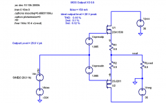
Below I have attached the schematic of my EC output stage using the Sanyo and Toshiba driver transistors.
Interestingly, I changed the transistors, tweaked the bias back to 150 mA, and ran the distortion without re-optimizing the EC trim resistor, and the distortion went up only very slightly from before.
Cheers,
Bob
Edmond Stuart said:
Hi Bob
The rationale behind different gate stopper resistors is quite simple. We don't need equal resistor values, rather equal time constants.
Generally, the effective gate capacitance of a p-channel mosfet is about 2.3 times higher than its n-channel counterpart, that is, if they both have the same trans-conductance, on-resistance etc. Why this is, I don't know exactly, but, considering that the mobility of the majority carriers in a p-channel mosfet (i.e. holes) is two to three times lower, I guess that the size of the chip is much larger, hence larger capacitances. (Ovidiu, please correct me if I'm talking utter nonsense)
With equal gate stoppers we get unequal common mode currents at the positive respectively negative going zero crossing transitions. At low frequencies this is not much of a concern, but at 20kHz it may increase the cross-over distortion and in case of a square wave it may even lead to a dangerous cross conduction of the two output devices.
In the picture below, I've exaggerated this effect just for clarity by using an unrealistic high frequency, i.e. 100kHz.
Red curves: equal gate stoppers, 150 Ohm.
Green curves: unequal gate stoppers, 100 and 240 Ohm.
Regarding your 'gate Zobels', indeed, it is a very nice and valuable trick. I hope you don't mind if I borrow your method to tweak my NFB-OPS.
BTW, my preference also tends to small-@ss xxx in the first place.
Cheers, Edmond.
Hi Edmond,
Thanks, this seems to be a nice explanation. I'll have to give it a try with some simulations.
Below I have attached the schematic of my EC output stage using the Sanyo and Toshiba driver transistors.
Interestingly, I changed the transistors, tweaked the bias back to 150 mA, and ran the distortion without re-optimizing the EC trim resistor, and the distortion went up only very slightly from before.
Cheers,
Bob
Attachments
Re: Re: Re: Re: hec != hoax ?
Thanks Bob.
In the mean time I've tweaked the NFB-OPS, a few caps more and lower gate stoppers. The schematic and gain/phase graphs are coming soon.
BTW, is your simulator still slow running with the EKV models? If so, you might replace the lengthy expression with tanh by a simple diode model between the gate and drain.
Cheers, Edmond.
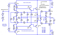
edit: Here is already the schematic:
Bob Cordell said:Hi Edmond,
Thanks, this seems to be a nice explanation. I'll have to give it a try with some simulations.
Below I have attached the schematic of my EC output stage using the Sanyo and Toshiba driver transistors.
Interestingly, I changed the transistors, tweaked the bias back to 150 mA, and ran the distortion without re-optimizing the EC trim resistor, and the distortion went up only very slightly from before.
Cheers,
Bob
Thanks Bob.
In the mean time I've tweaked the NFB-OPS, a few caps more and lower gate stoppers. The schematic and gain/phase graphs are coming soon.
BTW, is your simulator still slow running with the EKV models? If so, you might replace the lengthy expression with tanh by a simple diode model between the gate and drain.
Cheers, Edmond.
edit: Here is already the schematic:
Attachments
Re: Re: Re: Re: Re: hec != hoax ?
Edmond:
It would be nice if you could replace the ideal voltage bias sources with some real world circuitry. We both know from the PGP amp experience that this can be quite messy, for various reasons related to PSRR, noise, impedance, etc... Remember our PGP bias saga, starting with LEDs, going through noisy zeners and ending up with the LM369 low noise reference? I am not saying that the bias may fundamentaly change your OPS stage performance, but optimized bias sources (including temperature compensation) would certainly clearly reveal the real complexity of this OPS.
This is of course not rocket science (the 6.9V could be as simple as a amplified diode) but this has, of course, to be integrated and evaluated in the whole design. I know this is not really a sexy piece of work, but I think it's mandatory for showing a circuit that could be potentially built, rather than a textbook simulation exercise.
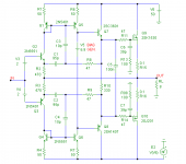
Edmond Stuart said:
edit: Here is already the schematic:
Edmond:
It would be nice if you could replace the ideal voltage bias sources with some real world circuitry. We both know from the PGP amp experience that this can be quite messy, for various reasons related to PSRR, noise, impedance, etc... Remember our PGP bias saga, starting with LEDs, going through noisy zeners and ending up with the LM369 low noise reference? I am not saying that the bias may fundamentaly change your OPS stage performance, but optimized bias sources (including temperature compensation) would certainly clearly reveal the real complexity of this OPS.
This is of course not rocket science (the 6.9V could be as simple as a amplified diode) but this has, of course, to be integrated and evaluated in the whole design. I know this is not really a sexy piece of work, but I think it's mandatory for showing a circuit that could be potentially built, rather than a textbook simulation exercise.
Re: Re: hec != hoax ?
Hi Bob,
Now the gain and phase plots look completely different. For example, the 1dB gain bubble has gone and the phase shift is far less due to the smaller gate stoppers. Interestingly, when I remove the compensating cap C10 (39pF) in your original schematic, your OPS also has a small gain bubble (0.5dB at 3MHz).
In order to create a playing level field, I've used the same transistors in your OPS as in mine, so the fast 2SC3601/2SA1407 as driver and for all other BJTs 2N5401/2N5551. The 95pF compensating caps might look funny, but at this value the Ft of the NFB loop gain is exactly the same as in your OPS. Needless to say that the gate stopper stuff is also identical.
The phase lag at 10 MHz has improved from 70 to 40 degrees and, if you don't mind, it is even slightly better than HEC.
And the distortion, HEC: THD20=70ppm, NFB: 55ppm (BW=200kHz).
Cheers, Edmond.
NB: red = HEC, blue = NFB.
Bob Cordell said:Hi Edmond,
You may get some surprizes when you simulate the whole amplifier, that's all I'm saying.
..........
it looks like you have moved your 3 dB bandwidth out to about 8 MHz, and you are now actually at about +1 dB peak at 2 MHz. Ultimately, you appear to have about a 1.5 dB peak at about 3 MHz.
It looks like you sacrificed some stability to catch up to my speed. Your phase lag at 10 MHz is about 70 degrees, while mine, shown below, is only 43 degrees. Frankly, I don't think yours looks all that good in comparison. The one I'm showing below is the same circuit I used earlier, but with the 2SC3601/2SA1407 and 2SC5171/2SA1930 transistors in it.
One of the nice subtleties about the EC circuit is that the compensation provided by C1 and C2 rolls off the EC feedback while providing a feedforward effect to the forward path, minimizing bandwidth loss and excess phase introduction by the compensation.
Cheers,
Bob
Hi Bob,
Now the gain and phase plots look completely different. For example, the 1dB gain bubble has gone and the phase shift is far less due to the smaller gate stoppers. Interestingly, when I remove the compensating cap C10 (39pF) in your original schematic, your OPS also has a small gain bubble (0.5dB at 3MHz).
In order to create a playing level field, I've used the same transistors in your OPS as in mine, so the fast 2SC3601/2SA1407 as driver and for all other BJTs 2N5401/2N5551. The 95pF compensating caps might look funny, but at this value the Ft of the NFB loop gain is exactly the same as in your OPS. Needless to say that the gate stopper stuff is also identical.
The phase lag at 10 MHz has improved from 70 to 40 degrees and, if you don't mind, it is even slightly better than HEC.
And the distortion, HEC: THD20=70ppm, NFB: 55ppm (BW=200kHz).
Cheers, Edmond.
NB: red = HEC, blue = NFB.
Attachments
Re: Re: Re: Re: Re: Re: hec != hoax ?
Hi Ovidiu,
That's that certainly a good idea and I will implement them as soon as I'm finished with a new amplifier design, a low cost PGP.
Cheers, Edmond.
syn08 said:Edmond:
It would be nice if you could replace the ideal voltage bias sources with some real world circuitry. We both know from the PGP amp experience that this can be quite messy, for various reasons related to PSRR, noise, impedance, etc... .............
Hi Ovidiu,
That's that certainly a good idea and I will implement them as soon as I'm finished with a new amplifier design, a low cost PGP.
Cheers, Edmond.
Hi Edmond,
this last OS looks nice. I tend to interpret it as (sort of) a unity gain current feedback op-amp.
I simmed a somewhat similar stage with current feedback, but it's class A. In your schem one would need to add complementary EF's ahead and tap off the feedback from the output's sources, directly feeding into the emitters of Q2/Q3 via a gain set (closed loop) resistor. Thus, standing current would be set by the voltage offsets divided through the source R's, and no other biasing would be necessary. The source R's would be outside the loop, as I'm not the maximum damping factor camp, but they could be quite low, depending on bias currenz.
Actually I tried that with current feedback op-amps (and using bootstrapped supplies on these, which is a key point besides the cascodes) and got extremly low THD/IMD, sub ppm THD20 levels at full load and almost unmeasurable with LTspice at low drive and/or freq conditions (OK, class A is cheating). Quite successfully with different cfb op-amps and different bjt outputs I tried, now I'm about to replace the op-amps by simplified discrete circuitry
Should I start a new thread and elaborate on this? It's heavy feedback, after all...
- Klaus
Attachments
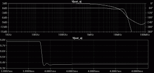
-143dB THD20 at 49W into 8 ohms resistive?THD: 0.000007%
traderbam said:
-143dB THD20 at 49W into 8 ohms resistive?
It is only a simulation
. In real life it would be VERY different. Some of many possible reasons for that would be non-linearity of the opamps and problems of matching between two halfs.Alex
ahem, it's 20Vp into 8ohms//50nF (clip limit is 5.5ohms), so it's only 25W with a 20Vp sine.
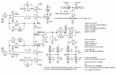
But the THD numbers are true... believe me, I really hesitate to believe it as well, mainly because the op-amp models all state "distortion not characterisized" (that's why I need to sim it with discretes, and build it). But, in fact when I sim the op-amps as simple followers with no load and 2Vp drive, I get more distortion from the op-amps alone! I tried THS6012+MJL3181/1302 and AD811+MJE15032/33. OTOH the op-amps run at optimal conditions: no common mode voltage and only little output swing, less than 300mV for the shown circuit. Also, the cascoding helped a lot. The stage is virtually isolated from the drive/output voltage, it only "sees" output current. Of course the design is not finished at any rate (not procection of any kind, won't like >0.5uF at the output), it's only a study so far...but the stunning numbers make me think I give i try, instead of fiddling around with chip amps biased to class A by the same method (which is how I came across the whole thing).
Blocks of this stage could easisly be parelleled (and bridged) to give more power and low load (2R) stability... also the front end biasing is easy to do with resistor dividers to (seperately regulated rails)
Attached is the .asc (renamed to .txt), the bjt models are those from andy_c and the THS6012 comes directly from TI.
- Klaus
Attachments
Klaus,Originally posted by KSTR But the THD numbers are true...
what happens in your simulation if you get some mismatch between R1 and R7 ?
Cheers
Alex
Hi Alex,
I've done this extensivly with an earlier version (op-amp supply referenced to output and without the cascodes), and found a sweetspot when slightly imbalanced (lower R on the PNP side). This might be due to the different intrinsic Re's in the NPN and PNP, resp.
I tried again now, same behaviour:
x was used in {R1*x} and {R7/x}, from 0.8 to 1.2 in steps of 0.1
- Klaus
I've done this extensivly with an earlier version (op-amp supply referenced to output and without the cascodes), and found a sweetspot when slightly imbalanced (lower R on the PNP side). This might be due to the different intrinsic Re's in the NPN and PNP, resp.
I tried again now, same behaviour:
.step x=0.8
DC component:0.0434077
Total Harmonic Distortion: 0.000015%
.step x=0.9
DC component:0.0206684
Total Harmonic Distortion: 0.000009%
.step x=1
DC component:-0.000166743
Total Harmonic Distortion: 0.000007%
.step x=1.1
DC component:-0.019027
Total Harmonic Distortion: 0.000007%
.step x=1.2
DC component:-0.0359612
Total Harmonic Distortion: 0.000010%
x was used in {R1*x} and {R7/x}, from 0.8 to 1.2 in steps of 0.1
- Klaus
syn08 said:
I have seen Bob's protection design, but unfortunately it did not pass my filters. Regular optocouplers do not match the speed requirements for the majority carriers injection time constants, so the protection effect is most likely only statistically effective (depending on the Vds when the short circuit condition occured). High speed optocouplers like the HCPL-772x from Avago Technologies with 40nS delay times would certainly work, but I could barely justify the cost of these very expensive devices.
Hi Ovidiu,
Could you elaborate on the opto coupler speed issue? In my protection circuit, the optocouplers are quite fast, as the sensor is a silicon transistor structure. Probably on the order of 1 us or better. Are you suggesting that a 1 us response time to shut off the gate drive to the MOSFETs is not fast enough in the event of a short circuit?
Thanks,
Bob
Re: Re: Re: Re: Re: Re: Re: Re: Re: Re: Re: Re: Re: Re: Error Correction Sensitivity
Yes, I think that is worth a shot. We'll look forward to your results. I think the matching helps a lot, and the lower required gate turn-on voltage is nice. I think they are about $5.50 in quantity of 10 at Digikey, if I recall.
Cheers,
Bob
syn08 said:
You guys brought me to the point I'll pull my wallet and purchase a stock of these devices from DigiKey, as Christmas gift, and do some real world measurements
The only special think I can infer from these devices datasheets is that they are N/P matched for transconductance rather than for various charges (which also explains Edmond's preference for different gate stoppers). This is why they, most likely, deliver better performance in linear applications, while the Fairchild/IRF/etc... are optimized for switching applications.
Yes, I think that is worth a shot. We'll look forward to your results. I think the matching helps a lot, and the lower required gate turn-on voltage is nice. I think they are about $5.50 in quantity of 10 at Digikey, if I recall.
Cheers,
Bob
- Home
- Amplifiers
- Solid State
- Bob Cordell Interview: Error Correction