As about the bootstrapped driver transistors I could use BC550/560 pair?
No, they have not enough power to charge the capacitances of the MOSFETs. And they can not mont at the Heatsink.
My choice would be 2SC5171/2SA1930 for example.
Need to check the SOA for the BC5x0 devices but the BC3x7 devices are certainly good enough.
The vce of the bootstrapped driver is very low and the SOA at this voltage is more than enough. There is no need to mount them on the heatsink from a dissipation point of view.
I have a bootstrapped driver (BC3x7-40) stage running two pairs of 20x20 Exicon MOSFETs with no problems. The MOSFET bias current is stable as would be expected from Lateral MOSFETs.
The speed up cap is optional. If you use one it needs to be about 5x the total capacitance of the MOSFET gates. Again, I would leave space for it on the PCB so you can experiment when you build a prototype.
Simulation is one thing but the real world shows up problems you don't see in simulation.
Have you thought about making the cascode in the LTP driven? For example off the LTP tail?
Also have you experimented with a small cap across the feedback resistor (R3)? Sometimes you can gain some extra PM this way.
Hi everyone,
Thank you for your help mcd99uk clarifing this questions,
Do you think that I have a low PM?
68º is not enough?
I can try your improvements.")
Low valued capacitor in parallel with the feedback resistor is used to reduce the peaking in common TPC, not in TMC I think
About your design what do you use to supress local oscillations in the OPS, gate/base stopper resistors, zobel networks from gate/base to drain/collector/gnd or both.
I'm thinking about using only base/gate stopper resistors.
I think that BC550/560 and BC3x7 have similar SOA characteristics.
Best regards,
Daniel Almeida
Thank you for your help mcd99uk clarifing this questions,
Do you think that I have a low PM?
68º is not enough?
I can try your improvements.
Low valued capacitor in parallel with the feedback resistor is used to reduce the peaking in common TPC, not in TMC I think
About your design what do you use to supress local oscillations in the OPS, gate/base stopper resistors, zobel networks from gate/base to drain/collector/gnd or both.
I'm thinking about using only base/gate stopper resistors.
I think that BC550/560 and BC3x7 have similar SOA characteristics.
Best regards,
Daniel Almeida
Thank you for replying gootee
What happens if you have less than 78º?
The slew rate with 78º will be much lower, I think.
With 78º I've much more THD.
I will have to use 150pF or more at TMC!!!
I think that not all amps have 78º, but it's a good phase margin indeed.
I think most amps have PM between 60-80º.
What I think is that not all amplifiers can have the "optimal" phase margin 78 degrees without some drawbacks, like lower SR.
Best regards,
Daniel
Last edited:
If the amplifier has 4 differently located compensations and each is optimised for the stage they are looking after, then the result is good.
If one or more of these compensations is NOT optimised and that stage/s introduces a high phase delay/error, then the other compensations will require to be set non optimally and thus set to introduce enough delay to "slow down " the amplifier sufficiently so that the total phase delay is OK for adequate stability.
The clever bit (that I have proved incapable of) is identifying those stages that need additional compensation and recognising how to optimise them.
Then the dominant compensation can probably be relaxed and still have a very adequate stability without excessively slowing down the amplifier. This is a "real" designer at work, something I will never be.
Last edited:
Hi everyone,
Thank you for replying.
That point of view seems interesting AndrewT, unfortunately I've never received formation about compensation in opamps. I'm currently taking a telecommunications and electronics BSc degree, but I don't have formation on that area, so I have to use known compensation schemes like conventional dominant Miller compensation (this one is good but has very low slew rate is used in the most commercial audio amps and opamps) , OPS inclusive Miller compensation (this one seems unstable I've never used, but many manufacturers uses this scheme in audio ICs with quasi complementary OPS), Miller input compensation (I don't know almost anything about this scheme, but seems "better" than conventional Miller compensation that turns the amp too slow), then we have TPC and TMC that are related, with TMC being a combination of TPC (two pole compensation) that has very good characteristics, with IMC (OPS Inclusive Miller Compensation proposed by Chery). There must be many more compensation schemes but I don't know them, but they could be even better. I'm also not a compensation schemes designer, unfortunatelly, a good compensation scheme it's a very important point in an audio amplifier design, because compensation affects BW, stabillity and slew rate.
Best regards,
Daniel Almeida
Hi everyone,
Talking about bootstrapped drivers again, I'm interested in using them, maybe with the BC550/560 pair or with 2N5551/2N5401.
It's a good idea to use a capacitor in parallel with the feedback resistor when using TMC?
If so what value I should use?
The IPS(TCS) cascode should be LTP driven? What are the advantages and disadvantages?
Best regards,
Daniel
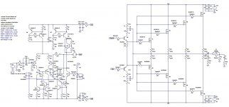
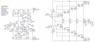
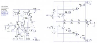
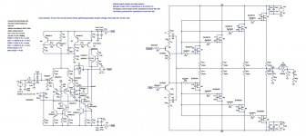
Attachments
Last edited:
Hi everyone,
I don't know if I'm making something wrong but LTP driven cascode at the IPS(TCS), have increased the THD characteristics when I tested it. If I put a capacitor in parallel with the fb resistor the PM increases indeed, but GM decreases, and a strange peaking will appear at OLG plot if this capacitor is of more than 10pF.
Best regards,
Daniel
Bootstapped drivers - if the BC5x0 transistors have enough current capability with a 12V Vce then they are ok. The Bc3x7-40s are available from mouser. Mouser is a cost effective way of getting parts and are quick to deliver (at least to the UK).
Feedback capacitor - I see no reason why you can't use it with TMC. Set your sim up for checking PM/GM and play with some small values and see the effect. watch out for increases in frequency of the 0db loop gain point.
Driven LTP cascade - Was playing with this idea last night and it appears a better way is to drive it off a replica of the feedback node. This is done by using a divider that is the same as the feedback network but with the replica shunt feedback resistor tied to a negative voltage. there is a diagram of this in Bob Cordell's book in the input stage section.
Hi everyone,
Thank you very much for your help mcd99uk,
I order the parts from Mouser too.
The capacitor in parallel with the fb resistor exchange gain margin for phase margin indeed.
I've noticed that open loop gain peaking occurs if I change the gate stopper resistor values, Why is that, with normal EF drivers this is less evident and only occurs if the values are lower, this peakings introduce nonlinearity in OLG and lack of gain margin
I Don't want to reduce this gate stopper resistors values, but why is that? I'm afraid because gate capacitance could be different from the one in the models in real world.
Talking about the fb capacitor again, I could use a 1-2pF cap, but I'm afraid that the phase will decrese for 10-11 degrees.
Could you please refer to the page and figure of Bob Cordell's book.
PS
Do you use any aditional network to keep the OPS stable in your design.
Thank you once more mcd99uk, and the other diyers that are helping me with this project,
Best regads,
Daniel
Last edited:
Bootstrapped drivers - don't have the answer to the peaking question. I wonder though whether we need to look at each stage of the amplifier and work out the frequency of pole they add. I recall reading somewhere (I think it was AndrewT) said that each amplifier stage must not be faster than the stage preceding it. (AndrewT, sorry if I'm wrong about this - memory must be distorted)
As for simulation vs real life, my thoughts are simulation is a starting point and a tool for learning the circuit. Then you know how to correct any problems encountered.
OPS stability - I only used gate stoppers and G-D ceramic caps soldered directly to the MOSFET pins. Exactly as magicbox detailed. I posted it on one of you other thread IIRC.
Driven cascode - Bob Cordell's Book Page 147 Fig 7.17.
Thank you very much for your help mcd99uk,
That peaking only appears when I use a lower gate stopper resistors value, with the values of 330ohm for N channel and 220 ohm P channel that are the values I'm using there's no sign of peakings in OLG.
About OPS satbillity networks, are you talking about "pure capacitor" from gate to drain or a zobel network from gate to drain?
What are the best values for this capacitor/zobel network.
Do I have to simulate the circuit with this additional network and check PM and GM.
Best regards,
Daniel
Hi everyone,
Thank you very much mcd99uk for all the help you're giving me,
I've modified the IPS (TCS) to a output driven cascode like mcd99uk suggested, and now the THD1 have dropped from less than 0.00002 % to less than 0.00001% when driving 100 Wrms into a 8 ohm load, which is just great
I've added a capacitor in parallel with the feedback resistor, and now I can adjust it to have more PM and suppress some peakings, to acheive this I have also added gate to drain capacitors to dump oscillations, like mcd99uk suggested, I've made simulations both using the gate stopper resistor values suggested by Semelab (in the app note attached) that are 330ohm (N) and 220ohm (P). I've also tried a combination with 2x lower gate stopper resistors 150ohm (N) and 100ohm(P). I've to change the GD capacitors accordingly, this slightly reduces THD20 but it's on the order of the ppm.
It's better to use the Semelab suggested gate resistors value (1MHz MOSFET BW), or the smaller values (2MHz MOSFET BW)?
Do you think I should use also base to colector capacitors or something similar in the drivers?
mcd99uk do you experienced some oscillation caused by the bootstrapped drivers? Do you added some network to supress it?
Best regards,
Daniel
Attachments
Hi Danny,
Looking good. I think you are probably over worried about oscillations due to the bootstappped drivers. I was using a diamond output and they are apparently more difficult to get stable. Didn't really notice this myself. All I had to do add a 10R resistor in series with the speed up cap. Never fully understood why though.
I question the use of the cascode VAS. If using the C3503 device as the second transistor in an enhanced VAS the benifets of the cascode are reduced. I remember michael kiwanuka proving that the miller compensated 3 transistor VAS had an unstable minor loop. I never see any meaningful improvement in THD when using a cascode over a non cascode enhanced VAS. The discussion between Mike K and Bob Cordell is buried in the Bob Cordell book thread.
I think that from a sound quality point of view there is not much difference between the values used for MOSFET gate stoppers. You would see improved stability margins from faster MOSFETs but that's about it. I using 1Mhz gate stoppers.
Have you tried simming into strange loads like capacitive up to 100n with no resistive element in series and without amplifier's output inductor. Try it see how close you can get to 100n.
PS. Try adding a small 30nH inductor to the MOSFET Drain connections to simulate 3 cm of PCB trace. Ensure this is right at the point where the Drain connections meet the power rail and leave the G-D caps eaxctly as they are. Then check for all the usual closed loop response and PM/GM.
Last edited:
Hi everyone,
Thank you very much for your great support mcd99uk,
I've changed the cascoded VAS for a simple one, the THD20 is mantained, THD1 raised from 0.00002% into 4 ohm at 200 W to 0.00004%, and from 0.00001% into 8 ohm at 100 W to 0.00003%, but I prefer this "normal" darlington VAS because it doesn't produce the peakings that the cascoded VAS produces.
I will use 330 and 220 ohm gate stopper resistors for the N, P devices respectivelly, to have a maximum frequency of 1 MHz.
I've tried purely capacitive loads, and with 10nF the things started looking darker, because GM reaches 6 dB, if I raise this value to 26nF, I've 45º of phase margin and 3-4 dB of GM, which are bad values, with more than 50nF the oscillation will be certain, because phase inversion around the loop occurs, indicating instability. I don't know if those are good or bad values, I don't know what I can do to improve them, what do you think?
I've also tried with the "normal" load adding the inductors at the supply per each MOSFET and the amplifier behaved normally, with more than 68º PM and more than 10dB GM, with values of inductance of up to 150nH, but a little more can be used without significant problems, what do you think?
Using supply inductors with less than 15pF G-D capacitors, problems will occur, and peakings are visible.
PS: I'm studying LM741 at college, do you know why they connect the dominant pole capacitor after the Vbe multiplier? I'm thinking about incorporating the circuit of figure 41 from Michael Kiwanuka's papers, what do you think? Good or bad idea? This circuit could influence GM/PM?
Thank you once more mcd99uk
Best regards,
Daniel
Attachments
Danny,
Firstly, with purely capacitive loads things will look very dark. The main thing is that the amp is still stable. I've had no problems with stability with an amp which could handle 68nF without output filtering. It has been stable in reality without an output filter. It will get one due course. Your PM/GM margins are adequate, mine has (simulated) GM = 60 degrees and GM = 14dB.
Try a small cap in parallel with the VAS degenerative resistor (22R). This can add to PM. In the order of 47pF to 4n7. It may send the amp unstable if too big.
Mike K's circuit 41 looks good however Rs could be better being a diode and connected directly to the driver outputs. This is where you'll be glad of using bootstrapped drivers.
Regarding the 741, not had time to work out the circuit. But you could move the TMC off the VAS output and on to the driver output. You would then have to make sure minor loop is still stable. This can be achieved by adding some lead lag shunt compensation to the VAS output. As long as this shunt compensation loads the VAS less than the TMC network would you should get some gains.
The test with the inductances added to the MOSFET supplies was to show you how PCB trace characteristics allow the G-D capacitor idea to work.
- Status
- This old topic is closed. If you want to reopen this topic, contact a moderator using the "Report Post" button.
- Home
- Amplifiers
- Solid State
- How to make a low distortion lateral MOSFET amplifier?