ESP - MOSFET Solid State Relays I built something like this and tested it. Nonlinearity of the MOSFETs' Rds(on) added about 0.003% THD at 100W, mostly third harmonic.
That is more distortion than mechanical relay contacts in good condition, but once they've got tarnished by city air and arced a few times, the MOSFET option looks more attractive.
I think I used the PVI1050 to drive it but it was a long time ago. Elliott writes about the need for a discharge circuit to turn the FETs off quickly, but the device I used had this built in.
Last edited:
Hi Danny,
Here you go. I have changed the models but that was only so I could run it on my pc. My mods to the schematic are a bit messy (not much spare time) but it gives you an idea of what to change.
Haven't done a detailed analysis but this looks stable under overload conditions.
Here you go. I have changed the models but that was only so I could run it on my pc. My mods to the schematic are a bit messy (not much spare time) but it gives you an idea of what to change.
Haven't done a detailed analysis but this looks stable under overload conditions.
Attachments
Photovoltaic drivers are like a solar panel and LED in a tiny package. They generate a floating voltage.
Whole thread is long but see post #260 amonst others. I did quite a lot of practical testing of these.
http://www.diyaudio.com/forums/solid-state/191449-output-relays-13.html#post2659578
And ChocoHolic who's idea was first put forward here,
http://www.diyaudio.com/forums/solid-state/155939-mosfet-relays.html
Hi everyone,
Thank you all for your great help,
Your articles are very interesting, scopeboy, what do you think I should use?
The IRF vertical mosfets?
Verticals are indeed faster that laterals, they while do a better job in a solid state relay, the optocoupler is connected to the thermal or offset comparator, right?
mcd99uk are you thinking about using something similar in your project?
Have you decided which devices you'll choose?
About the protection circuit, what's the purpose those 100R resistors connected to the source of the output devices?
Thank you once more for your help,
Best regards,
Daniel
Last edited:
Yes, solid state protection is what I am planning on using. I think I can cope with the distortion they add. Just the fact that can reliably break high currents at DC which small relays can't. Big relays can but i don't want such things due to cost and size.
Vertical mosfets are what I am planning on using. Don't need the thermal advantages of Laterals. All that's needed is low Rds ON and cheap devices. I am only at the beginning of researching how I'm going to do this. I will have +/-15V rails available anyway due to wanting to use a DC servo.
All the 100R resistors connected to each output device source is to allow all output devices to be monitored. What happens if you loose the device you are monitoring in original scheme? The rest get fried as the protection circuit is now effectively disconnected.
Minor loop stability, I'm still working on that one. All I have worked out is that you need to use tian probes. But what I'm struggling with is where to put the probe and how to break the loops.
The bad news for me is that suddenly the cascode enhanced VAS has given me a big reduction is THD.
Hi everyone,
Thank you very much for your fast reply mcd99uk,")
Yes I think I will go for the solid state relays too, the link that scopeboy posted has lots of good information
Vertical MOSFETs are made for switching applications in SMPS, so they give very good solid state relays.
I'm sorry for asking the same question, are you looking for some model of vertical MOSFET and/or optocoupler in specific?
A DC servo seems a good idea, it is good to prevent capacitor distortion present at the input and in the feedback path, do you think I should use one? If so what are the best opamp models, do you have the opamp models for LTSpice? TL081/2/4 are a good choice?
I'm sorry what is a tian probe?
Could you notify me when you have news about how to probe local stability?
What are the main transistor you are using at the VAS, with BC550 (using the cascode), I've 2x less THD1 at 4 ohm and 3x less at 8 ohm.
Thank you for modifying the circuit to supress the instabilities
I'm sorry but the circuit now limits the current at 4.8A per device for the P devices, and 6A per device in the N devices and the current limiting has a peaking, could you take a look? Please.
My goal is 6A per device, so N channel is protection is fine.
I'm sorry for bothering you with this.
PS:
You could use my Bob Cordell's models file, that includes the BUZ90x models.
With the output devices I'm using (BUZs), current limiting is up to 8A for the N device, which is unsupportable
For the N devices it's 5A.
Best regards,
Daniel
Thank you very much for your fast reply mcd99uk,
Yes I think I will go for the solid state relays too, the link that scopeboy posted has lots of good information
Vertical MOSFETs are made for switching applications in SMPS, so they give very good solid state relays.
I'm sorry for asking the same question, are you looking for some model of vertical MOSFET and/or optocoupler in specific?
A DC servo seems a good idea, it is good to prevent capacitor distortion present at the input and in the feedback path, do you think I should use one? If so what are the best opamp models, do you have the opamp models for LTSpice? TL081/2/4 are a good choice?
I'm sorry what is a tian probe?
Could you notify me when you have news about how to probe local stability?
What are the main transistor you are using at the VAS, with BC550 (using the cascode), I've 2x less THD1 at 4 ohm and 3x less at 8 ohm.
Thank you for modifying the circuit to supress the instabilities
I'm sorry but the circuit now limits the current at 4.8A per device for the P devices, and 6A per device in the N devices and the current limiting has a peaking, could you take a look? Please.
My goal is 6A per device, so N channel is protection is fine.
I'm sorry for bothering you with this.
PS:
You could use my Bob Cordell's models file, that includes the BUZ90x models.
With the output devices I'm using (BUZs), current limiting is up to 8A for the N device, which is unsupportable
For the N devices it's 5A.
Best regards,
Daniel
Attachments
Last edited:
Yes, when shopping for MOSFETs for your solid-state relay, you're looking for a voltage rating greater than the sum of your amp's rail voltages, and beyond that the lowest Rds(on) per dollar. The smaller the Rds(on) compared to the speaker load, the less of an effect any nonlinearity in it will have. There is a huge selection of cheap 200V MOSFETs in D2pak and TO220.
Bob Cordell's advice about using catch diodes after the relay as well as before is especially relevant. The inductive energy stored in a large woofer voice coil needs somewhere to go when the relay opens.
The optocoupler connects to the relay drive output of your protection circuit. The whole thing just substitutes for an ordinary speaker relay.
One advantage often claimed by lateral MOSFET fanboys is that they don't need complicated protection systems. Do you really need dual slope VI limiting?
The lateral MOSFET amp I built used it, but not the usual kind that clamps the audio signal, it was a separate circuit that would mute the audio and trip out the speaker relay if the overload persisted too long.
Last edited:
Danny,
The tian probe is explained in one of the LTSpice examples. I think it is Loopgainexample2.
I am currently doing some very basic reading on solid state relays. But currently concentrating on minor loop analysis as I see this as a block on further progress. Will let you know if I gain more understanding.
There is some question whether a DC servo is an advantage. Some say yes and others say not. One thing a DC servo does add is extra noise. I have used one in the working amp (TL072). I personally like them.
In my cascoded vas I have used the 2N device and got a good gain in the new design but no matter what I use in the working amp there isn't any change. Need to understand the factors involved more as manso stated in the Bob Cordell thread. Will try the BC5x0 later and see if there is any change in the new design.
As for the current limiting circuit. Try changing the 100R resistors to 10R and use the A1381 and C3503 transistors. This should work. I don't think there is enough current going to the bases of the protection transistors to turn them on hard enough. You may need to increase the caps in this circuit to keep stability since the resistors are now lower value.
Hi everyone,
Thank you mcd99uk and scopeboy for your great help,
This night I've discovered how to use the tian probe for checking for VAS stability, maybe you already knew how to do this
I've also discovered some changes that could be beneficial to increase VAS stability.
I've found out that my circuit with the cascoded VAS has 30º of VAS phase margin, and 60º with the beta enhanced VAS.
I've the explanation of the simulations and the changes that could be made to improve VAS stability in the LTSpice file attached.
I like to thank to mcd99uk, the LTSpice example really helped me
and to Michael Kiwanuka, I've used some technics of the test circuit he used in the discussion with Bob Cordell about VAS stability.
If you don't know how to probe VAS stability just take a look at my file and tell me what do you think, I'm interested in knowing your findings about how to make a more stable VAS.
Do you have the models for the servo opamp, mcd99uk?
What kind of circuit are you using, if it is one of Bob Cordell's designs, please can you say to me the figure and the page? Please.
Are you using a noninverting integrator, or two opamps, one with the inverting integrator and the other as the unity gain inverter.
I will try the improvements in the VI limiter circuit in the next night, I will try with the 2SC/2SA pair and with different capacitor values. This night was dedicated to VAS stability probing.
PS:
Phase margin at the VAS is seen with -180º as point reference, right?
For example if you have -150º at 0 dB you have a 30º phase margin, right?
Please, if you have time take a look in my files.
Best regards,
Daniel
Attachments
As a general rule, I would be wary of enclosing more than 2 transistors in the Miller compensation loop. Beta enhanced VAS is OK, but a beta enhanced cascoded VAS is 3 transistors. Returning the Cdom to the input stage makes it something like 4 or 5.
If you want to use more than 2 transistors, you should add a dominant pole to the inner loop you created.
If you want to use more than 2 transistors, you should add a dominant pole to the inner loop you created.
If you want to use more than 2 transistors, you should add a dominant pole to the inner loop you created.
This would make sense. I have found that when using a 3 transistor vas + moving the take off point to the pre-drivers that a 220pF shunt on the VAS output does the job, otherwise there appears to be an evil peaking in that minor loop. Doesn't meet the conditions for oscillation but nonetheless looks bad. As long as the ULGF is low then this shunt does not affect THD but does make stability margins worse. Suppose that this is because the VAS is now slower and adds more phase lag.
This has been the my experience too with trying to move the comp cap connection to enclose the input stage. From a global stability point of view everything looked good but when I try to run trans sims it oscillates like a beauty. The phase shift in the minor loop must be too great. Hence why I'm turning my education to the minor loops. I feel this is an important aspect to properly understand to allow progression to more advanced ideas
Lurking... enjoying the discussion and how the design is progressing.
Two thoughts, on the bootstrapped VAS, in a real world build the actual cap used will have a significant effect on the performance and how low you can get the distortion specs. Also, I don't know, but wonder how that bootstrap cap arrangement effects performance down to DC?
And the other thought which is probably not news at all is that those incredibly great simulated distortion specs? In a real world build, you won't get anywhere near that result. In order to eek out improvements you'd have to get into precise circuit trimming, matching/selecting devices and layout considerations.
I didn't really notice this, but what is the closed loop bandwith for the design? And do you have a slew rate or rise time figure?
You can look online, for Syn08, he has a highly optimized amp design on his website with details of the workup and circuit. He was a regular member here a while back. But it's worth looking at since it will give a good indication as to what is required to make a real world build of a design perform close to the simulated results...
EDIT: Oh yeah, forgot something... the mosfets in the output, usually the Nch and Pch input capacitance is different. So, you probably want them to end up the same, so any compensation cap sitting on the mosfet might be adjusted in value to reflect that. Also, in a real build, best to actually closely match the mosfets on a curve tracer - then you can drop the source resistors value or depending on just how brave you are they can be eliminated entirely.
Last edited:
Yeah. I've never bothered with Spice simulated distortion measurements. They are only as good as the Spice models of the parts you're using.
I remember Doug Self's series of articles that showed simulated plots of horrible crossover distortion in MOSFETs, but Bob Cordell showed that the distortion was only in the model. Real power MOSFETs have a subthreshold region that gives them quite different (better) crossover behaviour, and Cordell showed how to take account of this in LTSpice.
When I used the Exicon lateral MOSFETs, I remember the input capacitance of the P-channel devices was about twice that of the N-channel ones. I think I ended up with 200 ohm gate stoppers on the N-channel side and 100 ohms on the P-channel side. You can never get an exact complementary pair of MOSFETs because holes are less mobile than electrons. One parameter will always be different.
Parting thought: You probably won't hear the difference between 0.001% THD and 0.01%, but you probably will hear parasitic oscillations.
Danny,
I will have a look at your VAS stability tests tomorrow. Time has been limited today.
As for my findings (so far) the best method for stabilizing the VAS was to add shunt (lead-lag) compensation to its output. All other attempts have failed miserably.
The servo I'm using is the 2 op amp version from Bob Cordell's book page 160. But I've added a 220n cap across R7. This solved some oscillations I was getting from the servo. In Ltspice I use LT1128 but it really doesn't matter which one you use as long as its a basic op amp. The built in models are said to be inaccurate anyway.
Regarding the cascode VAS . Try the hawksford way. Move the LED connection from the power rail to the emitter of Q5 / Base of Q12.
Your L-FET emitter resistors can be as low as 0.2R for unmatched devices.
A good test for stability is to try and drive the amp with a big enough input signal to make it clip and then add a load to make it current limit at the same time into a Resistor // capacitive (100n) load. You may find some oscillations there.
PS. This was a quick "dumping" of thoughts before bed
Bear,
Regarding your comment about how the bootstrapped drivers act at DC. Obviously they'll struggle at DC but in real world tests I had no problems down at 10Hz sine waves. With the values Danny is using in his circuit he should be ok too. My real world amp has more than adequate bass response. For the bootstrapping caps I used panasonic FCs.
mcd99, I'm guessing that those are "audio" or low ESR electrolytics? I'd give you odds that you could hear them if you changed to mostly film in that spot, or some combination of films + an electrolytic, etc... guessing.
It's an interesting idea, the bootstrapped drivers, also wondering if they effect the phase margin any, since its a type of positive feedback, I expect.
Then too, I'm mildly curious as to what the amp does in response to a nearly DC signal while looking at the rest of the spectrum. Of course in normal use that set of conditions does not exist - but it could with LP playback.
_-_-
What about an active bootstrap circuit? Hmmm... lose the cap?
Hi everyone,
Thank you very much for your help, and for your interest in my project,
I really apreciate all the help you're giving to me.
I've a question to do to both of you scopeboy and mcd99uk, are you talking about the Douglas Self circuit of page 248, figure 8.6, with the points A and B?
If that's the case in point B you're including the input cascode transistors in Miller compensation loop, and that will look ugly, as you said scopeboy and I've confirmed, the minor loop is almost 2x more stable with a simple beta enhanced VAS compared to a 3 transistor VAS.
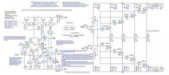
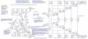
The solution you've purposed mcd99uk, seems good in improving minor loop stability, I don't know if I understand it well I've attached the minor loop Bode plots and a picture of the circuit with the shunt capacitor at the output of the VAS. The drawback are less PM and GM at the global loop and the decrease of the step gain of the VAS minor loop by more than 10x (20dB).
About your questions, bear, the circuit's closed loop BW is aprox 150 kHz (-3dB), I'm not expecting to have those THD specs in real life, I'm expecting that it can go as bad as something between 0.001-0.01% for THD1 and 0.01-0.1% for THD20, but I don't really care about that, I just want to make an amplifier that makes a good sound and with the best THD figures I can get, but that's my first solid state project.
I don't exactly know how to calculate the SR, can you help me here?
The GD capacitor could have another values, but I don't really know if this will influence very much, I was thinking about using 22pF for N-channel and 33pF for the P-channel, but I've opted for use the highest value for both.
I'm using that source resistors value (0R33) because of the VI limiters threshold current.
I know that if reduce them, I'll get better DF, but that's a price I've to pay.
I thought that parasitic oscillations are generally between 1 MHz and 100MHz, that's when the parasitic capacitances have lower impedance. And I can't hear 1-100MHz unfortunatelly. Please, correct me if I'm wrong, the only oscillation that I know that can be heard is motorboating and similar power supply decoupling issues. The other sound is if the output transistors blow up if they are oscillating with a large amplitudes at high frequencies, but I think this is unlikely if you use base/gate stopper resistors and if you've good gain/phase margins, more than (45º/6dB), I would say at least (60º/10dB), but that's my opinion.
mcd99uk I've a few questions to do if you don't mind, are you still using TMC when using the lead lag scheme?
What are the THD figures of your working amp, have you measured them? I'm curious about that.
Have you used TMC and a beta enhanced VAS in your working amp?
I will test your servo in my amp tomorrow, and I'll post the results of the Hawksford connected VAS, and of the capacitive load tests.
I'm a bit hesitant about using a cascoded beta enhanced VAS, it has less THD, but is more unstable, and I don't know if I want to slow it down and wasting some gain to make the minor loop more stable. What do you think?
I will also test and post the results of the modifications you suggested (mcd99uk) to the VI limiter.
Thank you all for your help and concern,
Best regards,
Daniel
Thank you very much for your help, and for your interest in my project,
I really apreciate all the help you're giving to me.
I've a question to do to both of you scopeboy and mcd99uk, are you talking about the Douglas Self circuit of page 248, figure 8.6, with the points A and B?
If that's the case in point B you're including the input cascode transistors in Miller compensation loop, and that will look ugly, as you said scopeboy and I've confirmed, the minor loop is almost 2x more stable with a simple beta enhanced VAS compared to a 3 transistor VAS.
The solution you've purposed mcd99uk, seems good in improving minor loop stability, I don't know if I understand it well I've attached the minor loop Bode plots and a picture of the circuit with the shunt capacitor at the output of the VAS. The drawback are less PM and GM at the global loop and the decrease of the step gain of the VAS minor loop by more than 10x (20dB).
About your questions, bear, the circuit's closed loop BW is aprox 150 kHz (-3dB), I'm not expecting to have those THD specs in real life, I'm expecting that it can go as bad as something between 0.001-0.01% for THD1 and 0.01-0.1% for THD20, but I don't really care about that, I just want to make an amplifier that makes a good sound and with the best THD figures I can get, but that's my first solid state project.
I don't exactly know how to calculate the SR, can you help me here?
The GD capacitor could have another values, but I don't really know if this will influence very much, I was thinking about using 22pF for N-channel and 33pF for the P-channel, but I've opted for use the highest value for both.
I'm using that source resistors value (0R33) because of the VI limiters threshold current.
I know that if reduce them, I'll get better DF, but that's a price I've to pay.
I thought that parasitic oscillations are generally between 1 MHz and 100MHz, that's when the parasitic capacitances have lower impedance. And I can't hear 1-100MHz unfortunatelly. Please, correct me if I'm wrong, the only oscillation that I know that can be heard is motorboating and similar power supply decoupling issues. The other sound is if the output transistors blow up if they are oscillating with a large amplitudes at high frequencies, but I think this is unlikely if you use base/gate stopper resistors and if you've good gain/phase margins, more than (45º/6dB), I would say at least (60º/10dB), but that's my opinion.
mcd99uk I've a few questions to do if you don't mind, are you still using TMC when using the lead lag scheme?
What are the THD figures of your working amp, have you measured them? I'm curious about that.
Have you used TMC and a beta enhanced VAS in your working amp?
I will test your servo in my amp tomorrow, and I'll post the results of the Hawksford connected VAS, and of the capacitive load tests.
I'm a bit hesitant about using a cascoded beta enhanced VAS, it has less THD, but is more unstable, and I don't know if I want to slow it down and wasting some gain to make the minor loop more stable. What do you think?
I will also test and post the results of the modifications you suggested (mcd99uk) to the VI limiter.
Thank you all for your help and concern,
Best regards,
Daniel
Attachments
Yes, I am referring to the scheme where the input stage is cascoded and the feedback goes through the cascode. Way too many transistors in there. :O
Parasitic oscillations aren't audible directly, but they can get into other parts of the circuit and get rectified by transistor junctions. This basically turns them into distortion.
When I used the lateral MOSFETs, I found that even with gate stopper resistors the amp was completely unstable. It needed a Zobel network. This had been left out of the schematic I was copying, and as a newbie I didn't realise that just about every power amp needs one in practice.
You said this is your first solid-state project so I would strongly recommend starting with the basic Blameless topology. Nice and simple, not much to go wrong. With a hot biased lateral MOSFET output stage you should get something like 0.001% THD-1 and 0.01% THD-20.
Once you have something working on your bench, if you really feel that you want lower distortion, you can try adding improvements like VAS cascodes and TMC.
Last edited:
- Status
- This old topic is closed. If you want to reopen this topic, contact a moderator using the "Report Post" button.
- Home
- Amplifiers
- Solid State
- How to make a low distortion lateral MOSFET amplifier?