Bear,
Can't see a problem with a near DC signal with a 20k sine imposed on top. I'll run a sim tomorrow evening (It will take some time). But I have tried it in testing for stability in real life. I had a fair offset of around 5V DC at the amp output with a sine running just up to clipping with no problems.
You may hear a difference with films vs electrolytics but it may not be as significant as you think as transistors can reject distortion at their collectors. Paralleling films and electrolytics are not a good idea. You have the potential for resonance / oscillations with this arrangement.
Active bootstrap sounds interesting. Have you any ideas?")
Danny,
Not sure which self circuit you are talking about. I only have 5th edition of his book.
I would go for the cascode (or at least lay the PCB out for one, you don't have to populate it). I'm going for as cascode in the next amp. It's all about learning and overcoming the problems.
The working amp is using Edmond's DTMC (Variant of normal TMC). It has Lead lag on the VAS output and an enhanced beta VAS. I borrowed a couple of ideas from Edmond's designs. No idea of real world THD as I don't yet have the equipment or access to any.
Real world testing allowed me to get the amp stable without gate zobels or caps but there was a very low level oscillation (around 20Mhz) that was causing an extra 20mA to be drawn off the PSU. This was fixed with G-D caps.
You'll find my monster circuit that is my first attempt at solid state design here
http://www.diyaudio.com/forums/solid-state/236002-amp-design-attempt-number-2-simpler-24.html#post3608505
It's overly complex but has served its purpose in getting some basic principles right.
Paul
PS Scopeboy, it was my failed attempt at making a blameless that got me designing my own amp The failed blameless would oscillate as soon as the output was connected to anything. No amount of miller comp made it work. So I stripped the components back out and threw the PCB away. It's much more fun creating your own stuff even if its not as good
Can't see a problem with a near DC signal with a 20k sine imposed on top. I'll run a sim tomorrow evening (It will take some time). But I have tried it in testing for stability in real life. I had a fair offset of around 5V DC at the amp output with a sine running just up to clipping with no problems.
You may hear a difference with films vs electrolytics but it may not be as significant as you think as transistors can reject distortion at their collectors. Paralleling films and electrolytics are not a good idea. You have the potential for resonance / oscillations with this arrangement.
Active bootstrap sounds interesting. Have you any ideas?
Danny,
Not sure which self circuit you are talking about. I only have 5th edition of his book.
I would go for the cascode (or at least lay the PCB out for one, you don't have to populate it). I'm going for as cascode in the next amp. It's all about learning and overcoming the problems.
The working amp is using Edmond's DTMC (Variant of normal TMC). It has Lead lag on the VAS output and an enhanced beta VAS. I borrowed a couple of ideas from Edmond's designs. No idea of real world THD as I don't yet have the equipment or access to any.
Real world testing allowed me to get the amp stable without gate zobels or caps but there was a very low level oscillation (around 20Mhz) that was causing an extra 20mA to be drawn off the PSU. This was fixed with G-D caps.
You'll find my monster circuit that is my first attempt at solid state design here
http://www.diyaudio.com/forums/solid-state/236002-amp-design-attempt-number-2-simpler-24.html#post3608505
It's overly complex but has served its purpose in getting some basic principles right.
Paul
PS Scopeboy, it was my failed attempt at making a blameless that got me designing my own amp
The failed blameless would oscillate as soon as the output was connected to anything. No amount of miller comp made it work. So I stripped the components back out and threw the PCB away. It's much more fun creating your own stuff even if its not as good
Last edited:
Paul,
I actually haven't done any thinking, assuming I could do some, about an active bootstrap.
My first inclination is to consider something that would revolve around a current mirror that gets driven. Second thought is something that might be a variant on the Allison bias scheme. But quite frankly, in terms of design, I am spotty, my main advantage if I have one is being born long enough ago to have seen and read a lot of stuff over time, where some things flash vaguely in the back synapses of what passes for a brain. So, nothing specific that I can point to. In fact I kind of think that the idea of bootstrapped drivers is one that hasn't been fully explored - thus the proliferation of designs that required a separate and higher voltage supply for the driver stage in order to get the outputs fully driven.
I suppose in some cases the paralleled caps could be a problem, but I haven't run into that myself. Electrolytics just make for icky sound, especially in places like feedback loops, and the like. The better (audio) electrolytics exist because they do sound better.
I'd not count on feedback to "fix" too many ills.
_-_-bear
Hi everyone,
I appreciate your help,
This night was dedicated to VI limiter circuits, I will try to the other improvements tomorrow night, I've made the changes you suggested, mcd99uk, but it seems like the drivers are getting out of their SOA, the IC current is getting close to 700mA, and Pd is 600-700mW, so I've made two test circuits, one with the output VI limiter connected to the drivers output and with a local VI limiter to limit the Ic and Pd of the drivers, even with this mods Pd of the drivers is high (450-500mW), the Id current was succesfully reduced to 100-150 mA, I've also changed the Vgs max of the output transistors (max Vgs is now 10V), what are the vgs max values you're using in your Exicon lateral mosfets, mcd99uk? I think they are similar to BUZs. As I said this solution is acceptable, but it adds complicity to the circuit and it is not very stable while limiting, because it is dependent of two VI limiters (drivers and OPS), PM and GM remains unchanged, no peakings and the THD values are preserved
The other circuit that is more simple, uses only one VI limiter at the output connected to the VAS, but to prevent oscillations I've to use base-collector capacitors instead of base-emitter capacitors, that's not a very good solution, but it was the only way to tame the oscillations, without compromising the drivers safety, this circuit decreases phase margin to less 1º, but the amp remains stable and without any peakings.
If you have time, please, take a look at my modifications.
I like your amp, mcd99uk.
It's a CFA design, right?
It has bootstrapped diamond buffer, really interesting.
Why do you prefer the CFA designs?
PS:
I've reduced Rs resistors to 0R15, to have more DF.
I will take a look at Douglas Self's Blameless amp as you suggested, scopeboy
Best regards,
Daniel
Attachments
Essentially the Blameless is just the classic voltage feedback amp circuit with the following changes:
Emitter degeneration on the input stage.
Current mirror load for the input stage.
Beta enhanced VAS.
Monster electrolytic cap in the feedback network (Self proved the "icky sound" is mitigated by using a cap so big that hardly any audio voltage appears across it)
Full complementary output stage, either double EF or CFP.
It isn't rocket science and really shouldn't be too hard to get working. The circuit you're simulating qualifies as a Blameless already.
You can see my "Selfless Amp" at scopeboy.com/amps - it includes a fully worked out and tested dual-slope VI limiter. The only change I made to the design since publishing the schematics was to put a diode in parallel with Cdom to improve the clipping behaviour.
On the subject of oscillations, I've found that the output stage will sometimes oscillate all by itself. The stopper resistors between the VAS and the driver transistors are critical in keeping it quiet. I've always found the values by experiment. I start at 100 ohms and increase them until I don't see any parasitics when driving a reactive load. Then I increase them some more for luck
Last edited:
On the subject of oscillations, I've found that the output stage will sometimes oscillate all by itself. The stopper resistors between the VAS and the driver transistors are critical in keeping it quiet. I've always found the values by experiment. I start at 100 ohms and increase them until I don't see any parasitics when driving a reactive load. Then I increase them some more for luck
This is probably where I went wrong. But as a good side effect it got me into amplifier design. Prior to this I was building other peoples designs.
I like your amp, mcd99uk.
It's a CFA design, right?
It has bootstrapped diamond buffer, really interesting.
Why do you prefer the CFA designs?
Hi Danny,
Yes, my amp is a CFA. My second design is a CFB also. It's not that I prefer CFA designs from a performance point of view. I like the topology as it takes care of slew rate automatically and they are easier to compensate.
The diamond output stage is ok but I'm not sure it brings much extra to the table over a normal output stage. It does produce strange phase effects. Discovered this when I tried to attach it to magic Box's VAS. Impossible to compensate without adding excess THD.
Your issues with the drivers going outside there SOA is because you have very big bootstrap caps. It may be worth calculating what you really need. Yours are almost twice the size of the ones I have used and the ones I used are probably over kill already. Worth some thought.
Your second version of the current limiting circuit adds excess complexity for what it gains.
Have you looked at the folded drivers detailed in Cordell Page 239 Fig 11.6. This topology performs well in sims. You can still use small driver transistors. May be easier to implement current limiting too.
Hi everyone,
Thank you very much for your help mcd99uk and scopeboy,
This night was dedicated to the test of the VI limiters and folded drivers.
As about the folded drivers I've discovered that they seem to add lots of THD20
and when I use them it's also difficult to set up the quiescent current in the output devices, I've to use a very low 10ohm resistor at the VAS!! I think they are intended to use with vertical MOSFETs not with laterals, I also have assimetrical current limiting when using the single slope VI limiter, almost no current enters the N transistor of the VI limiter and I can't understand why, if you want you can check my circuit to see if I done something wrong.
Talking about VI limiters, I've found out that in my design I really need something to protect the drivers even if I use 100u bootstrap capacitors, so I only see two options or I use a circuit to protect the drivers that it's working but with some oscillations, or I've to use a VI limiter connected to the VAS, but I'll have to use base to collector capacitors, and that's not good for PM, can you help me here?
Do you had the same problem in your amplifier mcd99uk?
In my previous drivers design where I've a pair of MJEs the current limiting can be sucessfully made using a VI limiter similar to the one you used in your circuit also with base to emitter caps, but connected to the VAS.
PS:
I've also tested a very, very simple CFA amp, but it's really bad, I've taken some ideas from one circuit I've seen from Analog Devices, it's a common CFA, but the performance is really bad, with very high THD, and a very bad output excursion, I don't know how to adjust the quiescent current in the output devices, the phase margin seems good, but the compensation is strange, I also want to make a CFA design later, my priority is making this VFA amplifier, but I also want to design a CFA to build later, but I don't know much about CFA, there are any books or papers that I can look at to take some inspiration. I don't want to just copy one design. Can you help me? Please.
Best regards,
Daniel
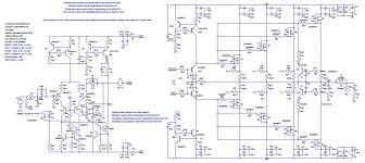
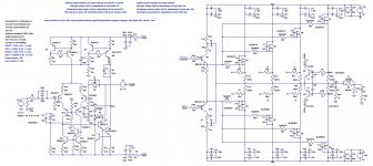
Attachments
-
 CFA_test.jpg195 KB · Views: 294
 -
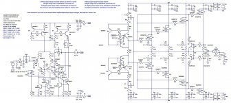
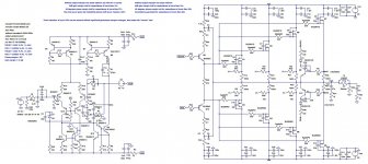
 amp7_tmc_hb5_bd10_prot2_3.jpg235.5 KB · Views: 293
 -
Cordell Models.txt19.2 KB · Views: 39
-
CFA_test.asc24.7 KB · Views: 37
-
Amp7_tmc_hb5_s_fd.asc28.2 KB · Views: 32
-
Amp7_tmc_hb5_s_bd10_prot2.asc28.3 KB · Views: 33
-
Amp7_tmc_hb5_s_drivers_prot.asc25.7 KB · Views: 32
-
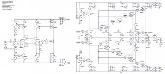
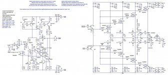 amp7_tmc_hb5_drivers_prot.jpg216.4 KB · Views: 277
 -
 amp7_tmc_hb5_fd_prot_.jpg247.4 KB · Views: 69
Last edited:
....fully worked out and tested dual-slope VI limiter.
Scopeboy,
Have you any plots of the VI locus against SOA curve, and calculations you used, to derive your two-slope component values?
Brian.
Plots here: scopeblog Blameless short circuit protection These were derived from pulse testing into an 0.1 ohm load while adjusting the rail voltage. The finished amp uses two pairs of output transistors, so the current axis is doubled.
I started with the component values published in Self's book and tweaked by simulation in LTSpice.
I started with the component values published in Self's book and tweaked by simulation in LTSpice.
Danny,
Have had a quick look at your folded driver asc file. Look at the current draw off the VAS into the drivers that gives you a clue as to what the problem is.
Add an EF stage to make it a triple to reduce load on VAS. Then you can bias things properly. Haven't looked at the implications of making this a triple with regards to stability but THD drops nicely.
The current limiting should be connected to the bases of Q19 and Q21.
Regarding your bootstrap problem. Change drivers to BC3x7-40 and then you will have sufficient SOA.
Hi everyone,
Thank you very much mcd99uk, you helped me a lot,
This circuit seems really good for the VI limiter, the current limit threshold is very simple to set, I've changed the source resistors to 0R15 to have more damping factor and to limit current to about 5A per device, but I noticed that I have a problem because Vdd is 50V and the current is 5A, so have 250W of dissipated power for each MOSFET and they can only have 125W, but if I limit the current to 4A or less I will have much less output excursion when using a real world 4 ohm speaker, how can I solve this problem I don't want to use more than 4 pairs of devices. Can you help me here.
The disadvantages of the folded drivers circuit are less phase/gain margins, and the THD1 is higher, as about capacitive driving, I can only drive 27nF without resistor in series and 47nF with a 0R1 resistor in series with the test capacitor.
I really wanted to use the bootstrapped drivers but I don't have the BC3x7-40 LTSpice models, can you give them to me? Please.
I've made a very simple CFA amplifier, just because I want to know more about this type of amplifiers, but this amplifier has lots of problems, can you help me here? Please.
I wanted to learn more about CFA amplifiers, do know if there any books or papers about this interesting type of amplifiers?
PS: I don't need to connect the VI limiter to the bases of the current source transistors, because the current is imposed by the current source, when the output is shorted all the current supplied by the source is drawn by the VI limiter transistor.
Best regards,
Daniel
Attachments
Danny,
The following is just some food for thought...
You could use natural current limiting detailed in Cordell Page 238. The bad news is that its not going to be completely symmetrical and you'll need to increase the VAS degeneration.
Thinking about the DF factor, are you worrying too much about this? 4 * 0.15R in parallel is 0.0375R and 4 * 0.33R in parallel is 0.0825R. What is the total resistance of the speaker wire and all connections between the amp output and speaker?
Your output stage has a total power dissapation of 8*125 = 1000W. This will equate to a capability of about 250W total output power. (Using a divide by 4 rule of thumb that has been suggested elsewhere and agrees with what I ended up designing for in my amp)
250W into 4R = I = 7.9A total. This suggests you need to current limit to about 2A per device at DC. Music isn't DC so you could limit at a higher current. Also, don't forget that the L-FET does a certain amount of self protection due to its thermal properties.
Could you current limit using the power rails? You could have a "sense" resistor in there and some sort of circuitry that shuts down or disconnects the output stage when too much current is drawn from the supply.
For CFA info, look at the CFA thread, Edmond Stewart's web page for design examples, Dadod's creations are very good as are Bonsai's. There doesn't seem to be a great deal out there so a lot is experimentation.
Attached are models for the BC3x7-40 devices.
Don't you just love amp design. It's all about compromises. This is what engineering is about, it's all a challenge.
Attachments
Sorry if I'm missing something obvious, but what is the point of the bootstrapped drivers? They won't drive the MOSFET gates outside the supply rails. Emitter followers have a gain of 1, so the voltage swing is still limited by the VAS.
The big advantage for me is that you can get away with using very small fast output devices. I would use the A1381/C3503 devices if they were available in the same Hfe rank. I know you could dig around in the grey market but I'm too cynical with regards to fakes.
It also meant that the current limiting circuit and all associated output components would be under less stress during current limiting. The only time the components would be under any stress would be the time that it took to discharge the bootstrap cap.
Another small advantage is that the gate zeners were no longer required.
So are you saying the plan is to limit the average current in the driver transistors with resistors in the collectors, and then use the bootstrap capacitors to give them a small local store of energy, so they can still deliver high peak currents and push the MOSFET gate capacitances around quickly?
Makes sense I guess, but if that is the plan then the capacitors only need to be something like 10 or 100 times the input capacitance of the output stage. I think Danny has like 1000uF in there, which would defeat the whole purpose as it holds enough energy to blow up the transistor.
I also don't see how it avoids the need for gate zeners. The gate insulation could still get degraded by short pulses of overvoltage.
Scopeboy,
You're summary is about right considering that the mosfet drive is just charge being shifted about and not currents like BJTs.
I like to think of the bootstrap from a voltage point of view. The voltage of the bootstrap is tied to the output voltage and this moves with the output voltage. Just trying to understand how the short pulses of over voltage could happen. Not saying they can't happen. Its something worth further consideration. If it can be determined they are required I'll add them in to my amp.
The bootstrap method just seemed like a neat solution during the design of my amp. It came about when considering current limiting. With a standard driver setup dumping all the drive current through the SOA protection circuit meant having quite a beefy driver setup and all associated components.
You estimate of the cap value sounds about right.
CFA amp info --
There are sources of information given in the recently closed thread on CFA design and the design results in SIM and actual circuit (from Elantec). Plus circuit developments by members here. Its a great topology which needs more flushing out to get the best from them. If you can find it -- also given in the CFA threads... a complete and detailed description including better SIM/spice topology than using old or vfa modified sim topology... -- " Emerging techniques For high frequency BJT Amplifier Design"... A Current-Mode perspective... by C.Toumazou and J.Lidgey and A. Payne. Sponsored by IEEE Circuits and Systems Society. Authors are from the UK. There you will get the accurate info... not here at Diyaudio.
A simplified version -- I call a complementary push-pull is also shown in my Headphone forum -- very simple circuit with -120dB distortion. That's measured... not a simulation.... into a real headphone for a load. But it has limited output and not for being a line stage to a power amp...-just to drive headphones to clean, loud levels. Similar topologies were started in 1980... see TAA magazine. I am also the inventor of the dc-servo circuit as used today to allow such circuits to exist as direct coupled-designs. Though the headphone amp does not need it, yet is direct-coupled.
Thx-RNMarsh
Hi everyone,
Thank you very much mcd99uk, you helped me a lot,
I've made a very simple CFA amplifier, just because I want to know more about this type of amplifiers, but this amplifier has lots of problems, can you help me here? Please.
I wanted to learn more about CFA amplifiers, do know if there any books or papers about this interesting type of amplifiers?
Best regards,
Daniel
There are sources of information given in the recently closed thread on CFA design and the design results in SIM and actual circuit (from Elantec). Plus circuit developments by members here. Its a great topology which needs more flushing out to get the best from them. If you can find it -- also given in the CFA threads... a complete and detailed description including better SIM/spice topology than using old or vfa modified sim topology... -- " Emerging techniques For high frequency BJT Amplifier Design"... A Current-Mode perspective... by C.Toumazou and J.Lidgey and A. Payne. Sponsored by IEEE Circuits and Systems Society. Authors are from the UK. There you will get the accurate info... not here at Diyaudio.
A simplified version -- I call a complementary push-pull is also shown in my Headphone forum -- very simple circuit with -120dB distortion. That's measured... not a simulation.... into a real headphone for a load. But it has limited output and not for being a line stage to a power amp...-just to drive headphones to clean, loud levels. Similar topologies were started in 1980... see TAA magazine. I am also the inventor of the dc-servo circuit as used today to allow such circuits to exist as direct coupled-designs. Though the headphone amp does not need it, yet is direct-coupled.
Thx-RNMarsh
Last edited:
Hi everyone,
Thank you all for your help,
I will try to answer to all your posts,
I've tested both BC550/560 and BC337/327 and I've noticed that both devices could be endangered if the VI limiter are connected to their outputs, so I've decided to connect the VI limiter to the VAS thru the base stopper resistor of the drivers and the result seems very good. I still have the same problem because I'm limiting current to a little more than 3A, but I should be limiting it to less than 2A, with 3A current limiting I have 10x times more THD1 for a 4 ohm load at 200W, THD1 for 8 ohm load at 100W remains unchanged. I think that I really need a single slope VI limiter with a resistor connected to Vcc, like the Fairchild circuit of figure 1 present in Michael Kiwanuka's papers, this resistor senses the Vds(or Vce) of the device and limits the current to lower values when Vds is higher, and that's what I need, do you know how I should calculate the value for this resistor?
I think that the connections to the speakers has an impedance between 0R1 and about 1R, but I'm not sure about this.
I'm thinking about using a relay maybe the same used for thermal shutdown, to shutdown the supply when the current drawn is to high, with a threshold of 15-20 A.
I've a circuit based on dadod CFA amplifier, but THD20 is very high can you help me here.
CFA topologies seems facinating, but now my wave is VFAs.
I've simulated the circuit with the VI limiter connected to the VAS thru the base stopper resistors of the drivers, I've simulated the amp for 20kHz and 1kHz with normal load and load shorted (1 mohm), and I never had power dissipation higher than 350mW, which is acceptable, and the current is always less than 100mA.
I should use bootstrap capacitors of about 10-100n?
I don't see large collector currents at the drivers in the simulations.
Thank you very much for replying with valuable information, RNMarsh, the headphone amp that you've made seems to have a really low distortion figure, impressive. The DC servo seems a great idea, using a integrator to control the DC offset, using a DC servo avoids the capacitors at the inputs, which cause a great improvement in distortion figures.
Best regards,
Daniel
Attachments
-
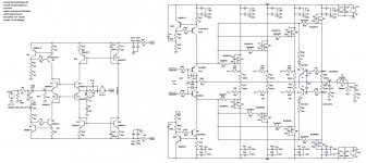
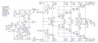
 amp7_tmc_hb5_bd10_prot5.jpg220.6 KB · Views: 227
 -
 amp7_tmc_hb5_bd10_prot4.jpg230.6 KB · Views: 232
 -
BC3x7_40 Models.txt1.2 KB · Views: 40
-
Fairchild Models.txt1.4 KB · Views: 44
-
Cordell Models.txt19.2 KB · Views: 39
-
CFA_test2.asc23 KB · Views: 34
-
Amp7_tmc_hb5_s_bd10_prot5.asc26.3 KB · Views: 34
-
Amp7_tmc_hb5_s_bd10_prot4.asc26.3 KB · Views: 35
-
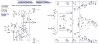
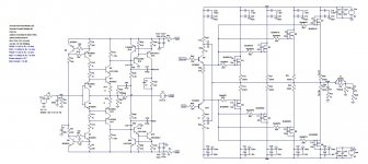 CFA_test2.jpg183.8 KB · Views: 225
Connecting the VI limiter after the driver transistor emitters makes no sense. They are designed to source lots of current so they'll just fight the limiter.
You have to connect it to the VAS because the current available here is well defined. In the positive direction, it is limited by the current source, and in the negative direction it is limited by a current limit transistor on the VAS (Q12 in your circuit) So the limiter can always "win" when it needs to.
The fundamental principle behind the current-feedback amp is that its input stage is powered by the feedback signal, not a constant current source, so it doesn't saturate when it sees a large error signal. The slew rate of a voltage-feedback amp is limited by input stage saturation, but the CFA topology removes this limit. This allows you to have a very high slew rate, or you can use the extra degree of freedom to optimise the design in some other way.
Of course in engineering everything is a compromise. If you want high slew rates in a CFA you have to deliver very high peak currents, and this makes current limiting and protection a challenge. If you're not careful, you end up with a circuit where every stage would fight your limiter until something blows. The audiophile "solution" to this is to leave out the current limiting altogether, which is just another compromise, trading reliability for ease of design.
- Status
- This old topic is closed. If you want to reopen this topic, contact a moderator using the "Report Post" button.
- Home
- Amplifiers
- Solid State
- How to make a low distortion lateral MOSFET amplifier?