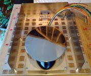
Beautiful. Sexy. A work of art. I have a hardware hardon.
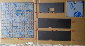
Are the threaded portions of your connectors perfectly circular or do they have flattened areas? It is usually too much work in DIY to make the holes with flats to match, but your lasered panel maker should be able to do it without charging extra. Something to consider for your next batch.
http://www.markertek.com/productImage/HI-RES/RJ-RWE.JPG
How do you ensure that there are no visible tool marks when you tighten the connectors?
In compact designs there always seems to be a tradeoff between compactness and serviceability. Quite often one has to do a lot of dismantling and reassembly to replace a faulty component. How much attention have you paid to this aspect of your design?
Thx!Beautiful...
No flattened areas and fully isolated from chassis.Are the threaded portions of your connectors perfectly circular or do they have flattened areas?
Careful mounting using high quality tools.How do you ensure that there are no visible tool marks when you tighten the connectors?
Maximum - to this new design.In compact designs there always seems to be a tradeoff between compactness and serviceability....
How much attention have you paid to this aspect of your design?
Great stuff. Looking very good. Thanks for the links. It's these little tips that help people a lot (on top of sharing the great amp design). I had previously wondered how to best mount a simple vertical shield within an enclosure.
Edit: what height is the enclosure? How many u?
Edit: what height is the enclosure? How many u?
Last edited:
As followers of this thread will know, with considerable help from Toni I have built his SA2014 in a dual mono configuration and have largely completed a single mono block version as well. As Toni's amps are all single-ended designs I had to construct a balanced to single-ended input board to interface with my balanced-only source signals. I built my version of Self's low noise unity gain balanced input stage (link). (With considerable help from other forum members I have explored advanced voltage regulator circuits. I have also built my own audio server powered by such. When a first started a few years ago I didn't really understand Ohm's law. )
)
However, I didn't want to just build the amps but rather also to fully understand the circuit design and choices made therein. My focus on this has been interrupted by an international move, but I now have some time while I sit down in New Zealand away from family distractions to return to it. The only text I have with me is Cordell. As I read it (again and again as it slowly sinks in) I keep a copy of Toni's schematics close by and continue to try to decipher them. I seem to be a slow learner of electronics...
While doing so I keep getting stuck on the VAS typology. When I look at the SA2013/14 schematic (rev 3.4.2-690) I can tick off a lot as "ok I get that". (Please correct any of the following if incorrect.) Input/AC decoupling network - check. Cascaded LTP - check. Loaded by current source (Q2, D1, D2 etc) - check. R14/R17 split and C10 added to filter the rail - tentative check? (Not sure of purpose of C6...) Input stage current mirror - check. Feedback network including C7 - check. Q11 (with D1 and D) provides current source for loading the VAS - check. The various forms of compensation available - check. Perversely having looked at feedback stabilization in voltage regulator circuits I find it easier to follow these than the VAS.
For the VAS, I see a Darlington configuration with Q9 driving Q12, but thereafter I am stuck. I have tried to reflect on the schematic versus Cordell's Fig 3.7 and I just don't understand where Q10 and Q13 fit in (versus his Q13). I have just unsure guesses at best on the rest. E.g. R25 helps turn off Q12 but I would have expected it to be connected directly to rail. (Same with R31 and Q13.) Even the purpose of C12 and C13 is lost on me.
I would love it if someone ever had the time to provide a detailed explanation of the VAS. Detailed for slow-coaches like me. Perhaps this will help other builders of Toni's amps better understand them as well. Hopefully it won't distract from Toni presenting his current build.
TIA
Steve
)However, I didn't want to just build the amps but rather also to fully understand the circuit design and choices made therein. My focus on this has been interrupted by an international move, but I now have some time while I sit down in New Zealand away from family distractions to return to it. The only text I have with me is Cordell. As I read it (again and again as it slowly sinks in) I keep a copy of Toni's schematics close by and continue to try to decipher them. I seem to be a slow learner of electronics...
While doing so I keep getting stuck on the VAS typology. When I look at the SA2013/14 schematic (rev 3.4.2-690) I can tick off a lot as "ok I get that". (Please correct any of the following if incorrect.) Input/AC decoupling network - check. Cascaded LTP - check. Loaded by current source (Q2, D1, D2 etc) - check. R14/R17 split and C10 added to filter the rail - tentative check? (Not sure of purpose of C6...) Input stage current mirror - check. Feedback network including C7 - check. Q11 (with D1 and D) provides current source for loading the VAS - check. The various forms of compensation available - check. Perversely having looked at feedback stabilization in voltage regulator circuits I find it easier to follow these than the VAS.
For the VAS, I see a Darlington configuration with Q9 driving Q12, but thereafter I am stuck. I have tried to reflect on the schematic versus Cordell's Fig 3.7 and I just don't understand where Q10 and Q13 fit in (versus his Q13). I have just unsure guesses at best on the rest. E.g. R25 helps turn off Q12 but I would have expected it to be connected directly to rail. (Same with R31 and Q13.) Even the purpose of C12 and C13 is lost on me.
I would love it if someone ever had the time to provide a detailed explanation of the VAS. Detailed for slow-coaches like me.
Perhaps this will help other builders of Toni's amps better understand them as well. Hopefully it won't distract from Toni presenting his current build.TIA
Steve
Last edited:
I will test it in the new amp with different standby power supply variants.
BR, Toni
I'm sure you haven't forgotten that it requires amendments to your output relay circuit.
...
For the VAS, I see a Darlington configuration with Q9 driving Q12, but thereafter I am stuck. I have tried to reflect on the schematic versus Cordell's Fig 3.7 and I just don't understand where Q10 and Q13 fit in (versus his Q13). I have just unsure guesses at best on the rest. E.g. R25 helps turn off Q12 but I would have expected it to be connected directly to rail. (Same with R31 and Q13.) Even the purpose of C12 and C13 is lost on me.
...
Q12 and Q13 are paralleled to increase the SOA when amp is clipping or output stage goes into current limit due to overload.
C12 and C13 help to increase the phase margin.
Ugh. That's a bit obvious now. Connecting R25 from emitter Q9 to base of Q10 rather than rail slightly lowers the voltage at which protection transistor Q10 kicks in? I guess I need to think more about why the base of Q10 is connected to the emitter of Q12 differently than the connection to its paralleled Q13. And then why the need for R29 and R30, ZD2 and D4. In the morning...
Answers (schematic from post 1145 and 1146):
- Q10 monitors the current through R26 to limit the maximum VAS current.
- We don't need to monitor the current through R32 because Q12 and Q13 are paralleled and matched. If Q10 collapses Vce of Q9 because of over current then transistors Q9, Q12 and Q13 are switched off.
- ZD2 limits the maximum Vce of Q9.
- R29/R30 limits the power dissipation for ZD2 and Q9.
- D4 avoids saturation of Q9 during clipping and thus reduces VAS "sticking".
Last edited:
Great stuff. Looking very good. Thanks for the links. It's these little tips that help people a lot (on top of sharing the great amp design). I had previously wondered how to best mount a simple vertical shield within an enclosure.
Edit: what height is the enclosure? How many u?
You are welcome!
Overall size is about 3U.
Heatsinks and case is exactly 120mm in height.
Frontpanel 130mm high.
Transformer totally oversized. 800VA and 8 x 35V secondaries.
BR, Toni
Thanks.
Ok I see that now. (Amazing how it now seems obvious.) What was the advantage of tying R25 (R31) to R26 (R32) instead of to the rail? I see it was in earlier iterations.
Which components are removed for "no VAS protection" performance measurements? Just ZD2? (I'm missing how the performance is slightly degraded by the protection.)
I went back through the first 250 posts or so. It is a real shame that the conversation was jumping between schematic and .asc references which were different and the schematic wasn't regularly updated. At the moment I can't go through it all with the .asc files open.
I noted the discussion regarding current mirror alternatives and that you went back to a simpler current mirror for SA2015. I also note you improved the current source from SA2014 by replacing 1N4148 D1 and D2 with a green LED (something I should retrofit into my SA2014 builds). Did you ever explore higher impedance alternatives utilizing a zener (or even low noise three terminal voltage reference) in lieu of D1 and D2 (or green LED)?
(BTW I note you changed the decoupling C14/15 of the rails to PWR GND as opposed to your original Sig GND. I still think I made a mistake on this with my balanced to single-ended input board. The op amp supplies there are decoupled to Sig GND...)
- We don't need to monitor the current through R32 because Q12 and Q13 are paralleled and matched. If Q10 collapses Vce of Q9 because of over current then transistors Q9, Q12 and Q13 are switched off.
Ok I see that now. (Amazing how it now seems obvious.) What was the advantage of tying R25 (R31) to R26 (R32) instead of to the rail? I see it was in earlier iterations.
- ZD2 limits the maximum Vce of Q9.
- R29/R30 limits the power dissipation for ZD2 and Q9.
- D4 avoids saturation of Q9 during clipping and thus reduces VAS "sticking".
Which components are removed for "no VAS protection" performance measurements? Just ZD2? (I'm missing how the performance is slightly degraded by the protection.)
I went back through the first 250 posts or so. It is a real shame that the conversation was jumping between schematic and .asc references which were different and the schematic wasn't regularly updated. At the moment I can't go through it all with the .asc files open.
I noted the discussion regarding current mirror alternatives and that you went back to a simpler current mirror for SA2015. I also note you improved the current source from SA2014 by replacing 1N4148 D1 and D2 with a green LED (something I should retrofit into my SA2014 builds). Did you ever explore higher impedance alternatives utilizing a zener (or even low noise three terminal voltage reference) in lieu of D1 and D2 (or green LED)?
(BTW I note you changed the decoupling C14/15 of the rails to PWR GND as opposed to your original Sig GND. I still think I made a mistake on this with my balanced to single-ended input board. The op amp supplies there are decoupled to Sig GND...)
Answers (schematic from post 1145 and 1146):
Have a look at post 914....What was the advantage of tying R25 (R31) to R26 (R32) instead of to the rail? I see it was in earlier iterations.
Removing of ZD2 would destroy Q9 - the small signal VAS transistor. Q10 is the current limiter transistor - this one has to be removed for this test.Which components are removed for "no VAS protection" performance measurements? Just ZD2? (I'm missing how the performance is slightly degraded by the protection.)
No. Using a green LED compensates the temperature drift of the two current sources.I noted the discussion regarding current mirror alternatives (...)
Did you ever explore higher impedance alternatives utilizing a zener (or even low noise three terminal voltage reference) in lieu of D1 and D2 (or green LED)?
Try to think of this "problem" as a Source feeding current into a Load and returning that current back to the Source......................
(BTW I note you changed the decoupling C14/15 of the rails to PWR GND as opposed to your original Sig GND. I still think I made a mistake on this with my balanced to single-ended input board. The op amp supplies there are decoupled to Sig GND...)
Now apply that to the supply rail. The HF transient current comes from the HF decoupling capacitor and goes into the amp/chip/processor and comes out.
Comes out to where? and follows what route? to get back to the source.
Completing that analysis of the current route should help you decide what traces need to carry the current.
It is usual for me to "simplify" the problem until it comes down to a level I can analyse. Try it.
Last edited:
No. Using a green LED compensates the temperature drift of the two current sources.
Ok. I don't follow the thermal argument. I do, however, note that your development sequence basically follows that discussed by Bob under Current Sources particularly Fig 2.10b to Fig 2.10c. He discusses the pluses and minuses of using a zener next (Fig 2.10d).
Try to think of this "problem" as a Source feeding current into a Load and returning that current back to the Source.
Now apply that to the supply rail. The HF transient current comes from the HF decoupling capacitor...
Perhaps I have this wrong but ... current is supplied to the circuit's op amps and returned via the negative supply rail. But is it right to think of these 100n caps as supplying HF transient power or rather as providing a low impedance path for HF rail noise away from the circuit or, in my case, away from the op amps? Ugh I'm getting confused.
My first iteration (and still accommodated in the second) followed Self's suggestion that it is normally sufficient to simply place the supply bypass caps across the supply rails. Toni's testing of that first board suggested otherwise and I added provision for caps to ground at the op amp supply pins as well. Unfortunately - I think - I routed them from supply pin to signal ground and not to the supply ground. A number of other routing changes were made also and we never retested caps across the rails again, but rather just used the caps to ground. The more I think about it I probably should have tested again caps across the supply rails or at the very least the caps should have gone to supply ground to provide a less circuitous path to the negative supply rail (rather than via the very indirect connection of signal ground to aux supply ground via the star ground).
Link to circuit
Last edited:
- Home
- Amplifiers
- Solid State
- 2stageEF high performance class AB power amp / 200W8R / 400W4R