A number of people's commented on the Ovation 250 that the VAS standing current was very high - a point I concede. This design is much lower, but I still prefer to run it 'rich'.
Seems the way to me. Ideally the transistor will be in it's Ft max operational area. That is usually a lot of current. Same for the IPS. And it reduces the V noise too. Some IC designer said for low noise - "use low impedances and crank up the IPS tail current 'til the silicon smokes"
I certainly plan to run the IPS and VAS near Ft max currents in my new amp. I have not actually seen this explicitly stated as an optimisation rule, can I claim it?
Best wishes
David
As pointed in your PDF symetrical differentials allow for 6db higher gain.
Due to the two sides working in parralel in AC mode noise is also
reduced by a 3dB factor compared to a single differential..")
As for current , well i use 1 to 2mA or so for the input differentials
and no more than 3mA for the VAS since this allow using low power
devices with very high gain that will reduce IPS loading even without
beta enhancer.
Due to the two sides working in parralel in AC mode noise is also
reduced by a 3dB factor compared to a single differential..
As for current , well i use 1 to 2mA or so for the input differentials
and no more than 3mA for the VAS since this allow using low power
devices with very high gain that will reduce IPS loading even without
beta enhancer.
Do you mean a triple EF where the predriver is actually a CFP pair (so 4 transistors)
or a CFP predriver(+driver) then EF output?
What was the instability and what did you try to stabilize it?
And this was not a simulation but a real amp with what transistors?
Best wishes
David
Its a triple ef where the prediver is a cfp. This caused high frequency oscilation. I tried caps accross B C on drivers and larger value base resistors for output transistors. With mosfet outputs the scheme using J200/k1529 worked without a glitch but with BJT I could get it stable. I tried this because I saw amps using darlingtons in this position although sims showed no real improvement. These were real time experiments, BJTs used were sankens 2sa2151/2sc6011.
Another scheme is the use of cascoded driver but not just any cascode, so called Hawksford. This I havent been able to stabilize either but it must be possible as Accuphase use it in their amps since 1990 upto now. This promises improved high frequency distortion which is where the problem really is.
I think running high IC for noise optimization and or selecting for Ft maximization are not new. IC designers do it all the time,
Of course they do. But I don't remember that Self or Cordell (or others?) recommend to check the Ft vs Collector current curve and try to run the transistor at the current that maximizes the Ft. Self just more or less routinely uses 3mA. For instance on a 2SC2547 (low noise) the maximum possible Ft can be improved by 270% over the 3mA value if the Ic is optimized.
This has the potential to improve stability or increase feedback.
Perhaps not relevant to simple Miller compensation but more so for input inclusive and similar advanced schemes.
So my heuristic (as Bob Cordell says) is to pick the collector current and then use that as a point to drive the design. It will determine the Re of course, and probably need a cascode on the IPS just to keep dissipation tolerable, for example. And it may even be a little more than optimum for noise, but it should be analysed not just lazily defaulted to some "traditional" value. To be fair to D. Self he does analyse this for noise but not Ft AFAIK.
And I like your term that you run "rich"
Best wishes
David
Last edited:
As pointed in your PDF symetrical differentials allow for 6db higher gain.
Due to the two sides working in parralel in AC mode noise is also
reduced by a 3dB factor compared to a single differential..
As for current , well i use 1 to 2mA or so for the input differentials
and no more than 3mA for the VAS since this allow using low power
devices with very high gain that will reduce IPS loading even without
beta enhancer.
Extra gain and less noise is a very attractive combination, isn't it?
Bode showed that the ultimate limit is the speed of the devices, so I plan to run fast then see about the consequences. An input cascode allows low power/excellent Hfe devices and still run plenty of current. A beta enhancer is fine too.
Best wishes
David
Interesting Homemodder. I never heard much about mirrors peaking as well (do you have link or can you point me in the right direction?). I am certainly now much more attuned to the possibility of these kinds of problems following mt experience with the cascode.
I would never have caught the cascode oscillation without my wideband scope BTW. Invaluable for audio
Its going to take me a little while longer to get the pages in electronic form. If you can, you could get the info from the following book.
Analog design, The current mode approach.
I agree if you run at currents that maximize Ft and minimize noise, you should be able to improve th design, provided other problems of course are not introduced.
Of bigger concern for me though is the behavior of the VAS stage with frequency (Cob) and the output stage hfe and Ft. Under heavy dynamic signals and a load that at any instant - due to the instantaneous frequency- may be at 2 ohms and the next at 15, there's a lot going on. You have Ft bouncing around all over the place (take a look at the Ft vs IC curves on the 1302/1381 or similar devices), hfe doing the same and of course, if the VAS transistor has not been selected carefully (or a suitable topology used), Cob is also varying, and along with it some of the parameters I already mentioned. So, the combo of these things creates quite a cocktail and a good design has to make sure none of them impact performance.
Of bigger concern for me though is the behavior of the VAS stage with frequency (Cob) and the output stage hfe and Ft. Under heavy dynamic signals and a load that at any instant - due to the instantaneous frequency- may be at 2 ohms and the next at 15, there's a lot going on. You have Ft bouncing around all over the place (take a look at the Ft vs IC curves on the 1302/1381 or similar devices), hfe doing the same and of course, if the VAS transistor has not been selected carefully (or a suitable topology used), Cob is also varying, and along with it some of the parameters I already mentioned. So, the combo of these things creates quite a cocktail and a good design has to make sure none of them impact performance.
Of bigger concern for me though is the behavior of the VAS stage with frequency (Cob) and the output stage hfe and Ft. Under heavy dynamic signals and a load that at any instant - due to the instantaneous frequency- may be at 2 ohms and the next at 15, there's a lot going on. You have Ft bouncing around all over the place (take a look at the Ft vs IC curves on the 1302/1381 or similar devices), hfe doing the same and of course, if the VAS transistor has not been selected carefully (or a suitable topology used), Cob is also varying...
Yes. it was a look at those 1302/1381 curves that made me think about this.
The maximum point naturally occurs where the slope is flat and so least sensitive to variations. Optimum value AND insensitivity is nice!
For an output this implies a quiescent that then drives the value of Re pretty low, limited by thermal stability mainly. A practical quiescent will be below the max Ft value so the number of output devices can be chosen so that at maximum load the current per device is at the maximum Ft value and this should move stability in the correct direction. Your amp looks nice in this respect.
Of course more quiescent and lower peak current will reduce the variation of practically any parameter. This is my idea on how to optimize this. It implies more current for the IPS, VAS and outputs than is commonly used and I am curious why.
Best wishes
David
Last edited:
Hello Algar,
I am not planning to make his PCB available.
There are two other amplifiers in the works. A 15W Class A current feedback amplifier (the sx-Amp) and an 80 watt class AB current feedback design (the nx-Amp). These will be with full PCB layout and write-ups on my website for anyone to build. However, please note it will still be a few months. I like to build and test before publishing. Please be patient. Thanks for your interest.
Hello Algar,
I like to build and test before publishing. Please be patient. Thanks for your interest.
Andrew, that is a novel idea, to build and test before publishing!!!
Last edited:
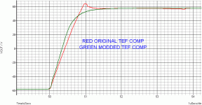
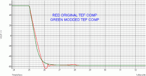
Hi Bonsai
Here some sims of the original TEF step response as well as those
of a slightly modded version.
The idea of the latter is to reduce pre drivers agressive capacitive loading
by implementing a local miller loop , a solution find in many japanese amps.
The mod apparently reduce bandwith in small signal analysis , although
phase margin seems better by 15°.
When checking the OPS in insulation , the modded version has in fact
better slew rate overall with more or less regular slope while due to
capacitive loading the original version exhibit a brutal reduction in slope.
The amplifier s step response with the two circuits , using only
two output pairs and 20R load :
Attachments
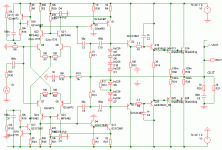
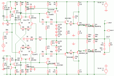
Wahab, looks like you put quite some effort into these sims. The networks between the bases of Q19 and Q28 and their associated rails in the diagrams above are not Miller compensation networks. They are damper networks, which along with the rail decoupling between Q19 and Q2 and Q11 and Q28 (not shown in your diagrams above) are designed to ensure that a Colpitts oscillator structure is not formed with the external circuit inductances. R1 and R9 (3.3 Ohm resistors) also aid in ensuring there is no parasitic oscillation in the output stage. I need to photograph the square wave response and post this up, but there is no overshoot on the final amp - note that the input filter is also part of the compensation network.
When looking at the compensation design, loop compensation has to be separated from parasitic prevention. The root causes of oscillation in these two areas are different.
I do measure slew rate with the filter disabled, but I don't think you can look at overshoot with part of the comp network (i.e. input filter) disabled.
In my write-up, note that when testing for squarewave response into an 8 ohm resistive load, this should be done by connecting the load before the output inductor - there should be no overshoot under those conditions. Again, when driving a normal load with expected capacitiance, then this is done with the load connected after the inductor and you can then expect to see ringing due to the tank circuit formed by the output inductor and the load capacititance.
Hello Nico. I used 2N5550/5551 for the cascodes and 547/557 for the LTP's. I chose the 547/557"s because of their very high gain, but of course they are not rated for the 65V rail, and that's why I cascodes them.
You do get improved HF supply rejection with the cascodes as well.
Actually, the original proto used 5550/5551 without cascading, but I I struggled to select pairs near the upper part of the hfe range. There are no issues with this of course with the 547/557 pairs. I'll need to take a look at te types you mention - I have not used them before.
- Status
- This old topic is closed. If you want to reopen this topic, contact a moderator using the "Report Post" button.
- Home
- Amplifiers
- Solid State
- Ovation e-Amp is Completed