Rhaaaaaa LC, do the #1615...i have to one more time to put my layout on eagle work bench......thanks for new schematic and "fonctionnel" confirmation.
Marc
It is basically the same as it was previously published, only some minor but necessary caps and trimmers added. At the end this is very high bandwidth design so the supply rails must be well decoupled at all crucial points. One of them is done by 1 uF cap as close to the output's collector pin as possible.
")
As you all guys already know I did a lot of extensive SSA testings and I am very familiar with this design, I know it better even than my pockets content, also all possible published versions are safely stored on my disks, so if somebody need certain info, just say it.
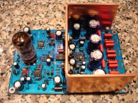
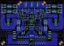
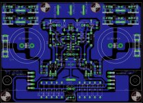
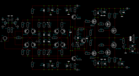
Today I finished the SSA BIGBT HP PCB layout & routing, so the files will be send to mine PCB manufacturer tomorrow morning. Only one question remains and still bothering me: which coating colour should I choose green, blue, red, white ... mhmmm
P.S. Maybe blue like my Projet Preamp PCB
Attachments
Last edited:
Ok,
LC i don't want to add the input offset controle as i've been sure the offset flows out my preamp. So just an input cap for foreigner occosional preamp. What mod should i do on you latest schematic?
Marc
Compare both schs and add some decoupling caps if needed, otherwise I think your version is OK. Anyway, please post your latest sch suited to your last PCB version and I can comment.
Anyway, please post your latest sch suited to your last PCB version and I can comment.
Here they are....
Attachments
Hi Idefixes
It will work with 2,2 kohm input impedance the same as with 10 kohm, depends only on your preamp's output current capability. Every value has its own benefits so you choose the one suits you the most, there is some room to experiment to get the best sounding solution in your system. I would certainly put two LEDs on board just to clearly see the normal operating conditions and/or fuses breakdown.
Input offset trimmer is almost a must if the amp is input DC coupled, so it serves to calibrate input offset (bases DC potential balanced to zero) when input is unconnected, so there is no change in an output DC offset if you short clamp the input or connect the zero DC low impedance source drive. We are speaking of some mV difference but anyway here's a possibility to trimm-out input DC offset completely to absolute zero conditions.
If you will use input coupling capacitor I have to inform you that it should be of high uF value at existing 2,2 kohm input to GND resistance. Just for an example input RC like 1 Mohm (input resistance to GND) and 1 uF (input coupling capacitor) means something like 1,6 Hz/-3 dB high-pass margin.
Also I would move 1 uF/0,1uF decoupling caps closer to the collector pins on PCB layout, just to prevent any HF ripple/oscillation loops over the supply rails. This is very important, cause I checked it just for the test purposes with my latest SSA HP VAS (small protoboard pictures) connected with 20 cm wires to the output stage. Immediately when I removed 1 uF decoupling caps near the outputs I got clear 17 MHz sine oscillation of several Vpp. This was also acid test cause I deliberately ran fully uncompensated amp on long VAS to output wires intentionally just to provoke all kinds of possible negative stuff to get the solution before PCB is made, so called stress tests.
All in all make small adjustments to PCB before going into production, now it is the time.
Regards, Andrej
Last edited:
Hi guitar
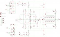
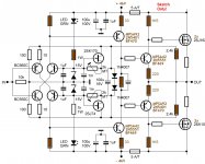
You can find all requested info in attached schematic. This one has all capacitors and other features needed for real world realization.
Thanks LC for the reply, but seems more things are added (as well as complexity)
what is the left top portion used for ? (Haven't saw such circuit before) and another set of voltage could be hard for me to achieve.
Could I ask why the you add another pair of 2.2k and 5k VR ?
The circuit main supply is written +-35V, is is compatible to +-40V too ?
What is the component labelled '5 A/T ', is it a fuse ?
I guess there are no special requirement for LED (even i can put RED, isn't it ?
)Do we need a input capacitor ? (seems most of the amp design have it )
If I were to make an power supply for it, at 40V how much capacity of reservoir should I prepare ? (asking for the power rating of this amplifier too)
So for those without voltage/power rating, I use above 50V & 0.5W is fine/sufficient ?
Just asking for fun, I have tons of BC550/560, could I make one SSA with all those ? (provided make it small output about 1W-5W)
Last edited:
Hi guitar
Quick answers:
- I am apologizing for that, no complexity, just well dressed TT version
- input DC offset nulling
- look very carefully +/- 15 V already present on both zeners
- fine adjustment for both halves - info on wikipedia
- it is
- 5 Ampere/Time lag fuse - info on wikipedia
- green LED colour means regular - normal operation, RED the opposite (alarm, faulty conditions, warning etc.)
- not mandatory
- calculate the Joules (energy), than calculate the Farrads (capacitance) - formula on wikipedia
- power ratings in Watt - formula on wikipedia
- different standards some 63 V, 0,66 W etc.
- yes you could
- BC-s are here because of their low noise, high hFE, high fT, etc. performance, not Watt-age, but you can try and smoke some plastic
Regards Andrej
Last edited:
Please repost all-corrected sch for the last inspection, regards, Andrej
LC
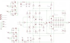
I opt. finally for this Basic - MosFet version of the SSA-Bal. If You think there would be anything to add to this chosen final, for better and more natural sound of Yours basic SSA-Mosfet version, than I would be more than happy for any suggestion, otherwise the "masters" confirmation is on the wish list.
Thank You,

Attachments
Thanks, Andrej. I kinda love short and quick answer.Hi guitar
Quick answers:
- I am apologizing for that, no complexity, just well dressed TT version
- input DC offset nulling
- look very carefully +/- 15 V already present on both zeners
- fine adjustment for both halves - info on wikipedia
- it is
- 5 Ampere/Time lag fuse - info on wikipedia
- green LED colour means regular - normal operation, RED the opposite (alarm, faulty conditions, warning etc.)
- not mandatory
- calculate the Joules (energy), than calculate the Farrads (capacitance) - formula on wikipedia
- power ratings in Watt - formula on wikipedia
- different standards some 63 V, 0,66 W etc.
- yes you could
- BC-s are here because of their low noise, high hFE, high fT, etc. performance, not Watt-age, but you can try and smoke some plastic
Regards Andrej
- What is "TT" stands for ?
- So should the +-15V of "DC input offset nulling" connect to point between zener & 1k 1W ohm resistor ? (each respective half )
- What is the maximum RMS of this design without much distortion ? So that I could give adequate reservoir.
- fried plastic sounds special.
Regards, Yang
Member
Joined 2009
Paid Member
DO you mean something like my draft attached ? (more output stages) Will this relieve the VAS somehow ? (the emitter resistor value is estimation only....)
Or is there any better implication ?
no, what you have there are two output devices in parallel with each other, the VAS collectors still have to drive the output devices directly.
My thought was to insert an extra emitter follower pair between the VAS and the output devices. Look at the output stage of some of the amps published on the forum, my TGM1,2 and 4, the DX amp series, the 'class AB amp for DIYaudio', etc.
I don't remember ever seeing a Class AB power amp with the output devices taken straight off the VAS collectors so I assume it's not recommended - I can't say I've tried it and that it doesn't work.
Hi guitar
You can find all requested info in attached schematic. This one has all capacitors and other features needed for real world realization.
I take this schematic as a reply to my question also in post #1596.
I have 5 pairs of 2SA1302/2SC3281 and 10 pairs of 2SA1837/2SC4793, purchased from MCM in 1997. I was planning to make Self's WW project. Those transistors are still with me unused.
To use the above, a thermally compensated bias generator is also required. As I intend use only +-35 Volts only, replacing the TTD diodes circuit with a suitable transister circuit as in post No 183 or 418 or 723 or 1005 may be required. Or may be like the one in 1449 with the transistor mounted on the heatsink. On the input side, a lp filter may be required. Can you kindly post a full diagram as SSA-BJT basic.
Can I use 1837/4793 in the place of BD 140/139 ? It is over kill, but I have those with me.
Thanking you for this wonderful thread,
--gannaji
for better and more natural sound
For so long I have not been able to describe the sound of such common drain output. "NATURAL SOUND". Hmmm... may be that would fit. I found that many people are attached very strongly to this kind of amp. I think Joachim also will like it
But why mosfet there, I don't like it. You can use TO-92 device to replace the mosfet. Something like this:
EDIT: Doesn't need double output stage for such a small amp.
Attachments
Last edited:
Lateral Versions
Problem is, there are so many possibilities with SSA, and this is amp is not "mature" enough yet. But LC already posted some basic circuits for some different types of SSA (ThermalTrack, BJT, Lateral, IGBT, BIGBT). Of course there could be others such as V-FET, JFET (Semisouth), Quassies...
For BJT, imo Bigun's triplet is the best. He has started a different thread for the SSA-TGM5 (and LC are also helping there).
For BIGBT, this main thread is the one, as LC is focusing more on this output stage.
For other types of SSA, of course somebody else may start another new thread. But without strong skill, who wants to do it? Better post here so many can help.
For Thermaltrack, Idefixes is in this main thread.
For lateral, besides a few "small" projects herein this main thread, there is SSA-Crescendo by Esperado.
From speaker building I have learnt that whenever "possible" start with the simplest circuit to achieve the "objective". Because complex circuit always has "unpredictable" effect that makes the design become difficult (to achieve acceptable performance by subjective ears). So here are what I consider from SSA-Lateral version (which is my favorite):
#1) Input Stage --> Lateral Output (Simplest SSA)
#2) Input Stage --> Input Cascode --> Lateral Output (Ruwe version)
#3) Input Stage --> (Input Cascode) --> TO-92 VAS/driver --> Lateral Output (Basic SSA)
#4) Input Stage --> (Input Cascode) --> TO-92 VAS --> TO-92 driver --> Lateral Output (Common Drain)
#5) Input Stage --> Input Cascode --> TO-92 VAS --> TO-92 driver --> Lateral Output (Common Source)
Option #1 is too simple to be useful. I prefer a class-A version if possible.
Option #2 is one of my favorite for low wattage amp
Option #3 is too general/common. I prefer to remove the input cascode, but front end regulator is a must, and it must be sophisticated (a.k.a Mosfet shunt regulator)
Option #4 is always a different animal. A somebody's pet.
Option #5 is my favorite for high wattage amp. Rail voltage must be high (note that the driver is emitter follower). Regulated front end supply may be needed to help stability (of course a mosfet shunt regulator). Tripple or double laterals. But double is enough because I insist the use of TO-92 drivers so power will not reach more than 100W I believe.
I suggest a fresh thread be started, for just this design, then all subsequent questions/answers can be on that thread only, and only that design will be discussed.
Problem is, there are so many possibilities with SSA, and this is amp is not "mature" enough yet. But LC already posted some basic circuits for some different types of SSA (ThermalTrack, BJT, Lateral, IGBT, BIGBT). Of course there could be others such as V-FET, JFET (Semisouth), Quassies...
For BJT, imo Bigun's triplet is the best. He has started a different thread for the SSA-TGM5 (and LC are also helping there).
For BIGBT, this main thread is the one, as LC is focusing more on this output stage.
For other types of SSA, of course somebody else may start another new thread. But without strong skill, who wants to do it? Better post here so many can help.
For Thermaltrack, Idefixes is in this main thread.
For lateral, besides a few "small" projects herein this main thread, there is SSA-Crescendo by Esperado.
From speaker building I have learnt that whenever "possible" start with the simplest circuit to achieve the "objective". Because complex circuit always has "unpredictable" effect that makes the design become difficult (to achieve acceptable performance by subjective ears). So here are what I consider from SSA-Lateral version (which is my favorite):
#1) Input Stage --> Lateral Output (Simplest SSA)
#2) Input Stage --> Input Cascode --> Lateral Output (Ruwe version)
#3) Input Stage --> (Input Cascode) --> TO-92 VAS/driver --> Lateral Output (Basic SSA)
#4) Input Stage --> (Input Cascode) --> TO-92 VAS --> TO-92 driver --> Lateral Output (Common Drain)
#5) Input Stage --> Input Cascode --> TO-92 VAS --> TO-92 driver --> Lateral Output (Common Source)
Option #1 is too simple to be useful. I prefer a class-A version if possible.
Option #2 is one of my favorite for low wattage amp
Option #3 is too general/common. I prefer to remove the input cascode, but front end regulator is a must, and it must be sophisticated (a.k.a Mosfet shunt regulator)
Option #4 is always a different animal. A somebody's pet.
Option #5 is my favorite for high wattage amp. Rail voltage must be high (note that the driver is emitter follower). Regulated front end supply may be needed to help stability (of course a mosfet shunt regulator). Tripple or double laterals. But double is enough because I insist the use of TO-92 drivers so power will not reach more than 100W I believe.
Last edited:
For so long I have not been able to describe the sound of such common drain output. "NATURAL SOUND". Hmmm... may be that would fit. I found that many people are attached very strongly to this kind of amp. I think Joachim also will like it
But why mosfet there, I don't like it. You can use TO-92 device to replace the mosfet. Something like this:
EDIT: Doesn't need double output stage for such a small amp.
Jay,
Thank You for Yours comment,
Mosfet vas for best uncompromissed driving the i/p capacitance of 2. fet OP pairs, which are there on purpose to drive with ease 2. OHm loads.
Kind regards
LC
I opt. finally for this Basic - MosFet version of the SSA-Bal. If You think there would be anything to add to this chosen final, for better and more natural sound of Yours basic SSA-Mosfet version, than I would be more than happy for any suggestion, otherwise the "masters" confirmation is on the wish list.
Thank You,
Hi SOUND_Rays
I finally found the time to look over your sch and here are the comments:
- T1 should be BC560C
- input offset trimmer's +/- 15 V is provided by the existing two zeners, if the tracks on PCB will be longer than 2cm than you should also decouple +/- 15 V DC rails with 1 uF caps close at trimmers side
- I suggest you to supply front-end with +/-45 V regulated PSU to make max efficiency from the output stage swing according to supply rails
- in this case change R10, R11 to 1,5 kohm/2 W
- driver's gate DC voltage is app. 8V, so I suggest to change R19 to 2,2 kohm and P4 to 1 kohm
- VAS loading impedance is very high, there is practically no fT limitation by the load and most probable point of local oscillation, amp is also without any freq compensation, so I suggest you to put in small local feedback compensating capacitor (10-22 pF, will be practically tested) between collector and base of T9, T10
I think now you're good to go.
Last edited:
Jay,
Thank You for Yours comment,
Mosfet vas for best uncompromissed driving the i/p capacitance of 2. fet OP pairs, which are there on purpose to drive with ease 2. OHm loads.
Kind regards
I think it is good to try this kind of output stage with drivers and outputs as mosfets. Pin layout of IRF's is adequate to standard TO-220 BJT so if there will be need to change the mosfet drivers to BJTs it will be like "piece of cake" (only some minor adjustments to Vbe multiplier).
Regards, Andrej
- Status
- This old topic is closed. If you want to reopen this topic, contact a moderator using the "Report Post" button.
- Home
- Amplifiers
- Solid State
- Simple Symetrical Amplifier